2 Diodes and Transistors
Introductory Example
Microcontrollers often have many pins that evaluate signals between $0...5~\rm V$ as a digital signal. However, the input signal can be disturbed during transmission by small coupled pulses, e.g. from HF sources like mobile phones. This interference can cause the signal to leave the permitted voltage range of approx. $-0.5...5.5~\rm V$ and thus destroy the logical unit.
To prevent such destruction, an over-voltage protection circuit consisting of diodes is installed (see e.g. ATmega 328). In case of an over-/under-voltage one of the diodes becomes conductive and lowers the input voltage by the resulting current. In the simulation, it can be seen that the interference on the input side can be reduced to an acceptable, low level by the protection circuit.
This chapter explains why a diode becomes conductive at a certain voltage, what has to be considered when using diodes, and which different types of diodes are available.
For the protection of digital interfaces that leave the device housing (e.g. USB), additional separate ICs are used that support this protection of the data processing chips. These protection diode ICs suppress the short-time voltages and are called Transient Voltage Suppressor or TVS diodes. Typical TVS ICs are NUP2301 or for USB NUP4201.
Further reading
- An introductory is available at electronics-tutorials
Objectives
After this lesson, you should:
- Know how to distinguish electron mobility in metals, semiconductors, and insulators,
- know what the intrinsic conductivity of a semiconductor is,
- distinguish between electron and hole conduction and relate them to P- and N-doping,
- know what doping is and what it is used for
- know the difference between real and ideal diode,
- be able to show the course in forward and reverse directions,
- be able to choose the correct diode from different diode types,
- be able to explain physical quantities such as reverse/residual current, reverse/residual voltage, and breakdown voltage.
2.1 Current conduction in semiconductors
Alternative to the explanation in the video
In metals, electrons are free to move. If an external voltage is applied, they follow the potential difference to the positive electrode: current flows. In insulators, on the other hand, the electrons are firmly bound to the atomic trunks. If a voltage is applied, they can at best be polarized. No current flows.
A semiconductor is a material whose conductivity lies between that of metals and that of insulators. The technologically most important example of a semiconductor is silicon. In the silicon crystal, the electrons are not freely movable as in metal, because they are bound to the atomic trunks. But a small supply of energy (e.g. thermal energy) is sufficient to release the electrons from the atoms. Then, when a voltage is applied, an electric current flows. This is called the intrinsic conduction (intrinsic conduction) of the semiconductor. When the electrons move around in the semiconductor, this is called electron conduction.
A hole with a positive electrical charge is created at the silicon atom from which the electron was removed. This is also called a defect electron. These holes can also move through the crystal lattice and thus generate an electric current. This is called hole conduction. Hole conduction can be thought of as a hole being filled by an electron from the neighboring atom. However, this creates a hole in the neighboring atom. Effectively, such a hole has migrated from one atom to another, carrying with it a positive electric charge.
Abb. 1: N-doping Abb. 2: P-doping
Most semiconductors are elements of the fourth main group, i.e. they have four electrons in the outer shell. This also applies to the element silicon. In the silicon lattice, each silicon atom is therefore connected to four neighboring atoms via a bond. If foreign atoms are added to this semiconductor material, the electrical conductivity can be modified. This is called doping.
Atoms of the fifth main group (e.g. phosphorus) have five electrons in the outer shell. If these are added to the silicon crystal lattice, one electron is surplus at these points, as it is not needed for the four bonds in the crystal lattice. This electron is much more mobile than the electrons that contribute to the bond and therefore greatly increases conductivity by electron conduction. This addition of free negative charge carriers is called N-doping (see Abbildung 1).
On the other hand, by adding atoms of the third main group (e.g. aluminum), a so-called hole can be created at these points, as these atoms only have three electrons in the outer shell. This leads to an increase in conductivity by hole conduction. This addition of free positive charge carriers is called P-doping (see Abbildung 2).
In metals, electrons are free to move. If an external voltage is applied, they follow the potential difference to the positive electrode: current flows. In insulators, on the other hand, the electrons are tightly bound to the atomic trunks. If a voltage is applied, they can at best be polarized. No current flows.
A semiconductor is a material whose conductivity lies between that of metals and that of insulators. The technologically most important example of a semiconductor is silicon. In the silicon crystal, the electrons are not freely movable as in metal, because they are bound to the atomic trunks. But a small supply of energy (e.g. thermal energy) is sufficient to release the electrons from the atoms. Then, when a voltage is applied, an electric current flows. This is called the intrinsic conduction (intrinsic conduction) of the semiconductor. When the electrons move around in the semiconductor, this is called electron conduction.
A hole with a positive electrical charge is created at the silicon atom from which the electron was removed. This is also called a defect electron. These holes can also move through the crystal lattice and thus generate an electric current. This is called hole conduction. Hole conduction can be thought of as a hole being filled by an electron from the neighboring atom. However, this creates a hole in the neighboring atom. Effectively, such a hole has migrated from one atom to another, carrying with it a positive electric charge.
Abb. 2: P-doping with aluminum
Abb. 1: N-doping with phosphorus
Most semiconductors are elements of the fourth main group, i.e. they have four electrons in the outer shell. This also applies to the element silicon. In the silicon lattice, each silicon atom is therefore connected to four neighboring atoms via a bond. If foreign atoms are added to this semiconductor material, the electrical conductivity can be modified. This is called doping.
Atoms of the fifth main group (e.g. phosphorus) have five electrons in the outer shell. If these are added to the silicon crystal lattice, one electron is surplus at these points, as it is not needed for the four bonds in the crystal lattice. This electron is much more mobile than the electrons that contribute to the bond and therefore greatly increases conductivity by electron conduction. This addition of free negative charge carriers is called N-doping (see Abbildung 1).
On the other hand, by adding atoms of the third main group (e.g. aluminum), a so-called hole can be created at these points, as these atoms only have three electrons in the outer shell. This leads to an increase in conductivity by hole conduction. This addition of free positive charge carriers is called P-doping (see Abbildung 2).
A Quantum Mechanical View
A deeper model of conductivity in semiconductors will now be considered in a little more depth. In the Bohr atomic model (Abbildung 5, 1), it is assumed that the electrons in the atom move in certain circular orbits around the nucleus - similar to the planets in the planetary system. Here, more strongly bound electrons are in closer orbits and weaker ones are in orbits further out. This also behaves similarly to satellites in the gravitational field, which, when farther from the center, are more weakly attracted. Bohr postulated 3 axioms to make the model and measurement results fit together plausibly:
- The circular orbits are discrete. There are only certain paths on which the electrons may move
(and thus: there are only discrete energies for the electrons). - Each „leap“ of an electron from one orbit to another is accompanied by an energy absorption or release.
- The exact energy of the orbits results from quantum physics.
Unfortunately, this representation produces quite a few physical contradictions - but the model is sufficient for explaining conductivity in semiconductors1). The Bohr atomic model and the Octet rule (the tendency of higher orbits to be saturated with 8 electrons) are enough to gain a deeper insight into semiconductor physics.
Abb. 5: Bohr's atomic model and band model
Abbildung 5 1a shows the electrons in the discrete circular orbits, i.e., in a (kind of) $x$-$y$ coordinate system. More strongly bound electrons are shown in yellow on inner orbits; on the outermost incompletely occupied black orbit, electrons are shown in blue. In addition to the occupied orbits, other, outer, non-occupied orbits are also present (green in Abbildung 5 1a).
The same electrons can also be sorted into an $x$-$W$ coordinate system (see Abbildung 5 1b). Here $W$ is the binding energy, or work released when an unbound electron jumps into the orbit under consideration. The origin of the binding energy (i.e., the binding energy of an unbound electron: $W = 0$) is above the unoccupied levels. Thus, as expected, the magnitude of the binding energy of the fully occupied level is the highest. The discrete orbits also result in discrete energy levels on the energy axis.
If we consider a section of a solid instead of a single atom, the electron configuration changes. In Abbildung 5 2a, the situation is again shown in the $x$-$y$ coordinate system. Here, the inner electrons and the nucleus are now reduced to a single, yellow circle with the resulting charges. The electrons from the (in the example atom) partially occupied levels now satisfy the octet rule.
However, depending on the element, there are different properties of the electrons here. In metals the electrons are freely movable - thus a good conductivity is measurable, but in semiconductors initially not. This statement cannot be explained by the Bohr atomic model, but by the band model and some quantum physics very well. As already for the atom, the electrons of the solid are now entered into a $x$-$W$-coordinate system. Here are now many electrons from the same atomic levels close to each other. The laws of quantum physics forbid that electrons occupy exactly the same energy level at the same location. This results in a broadening of the discrete levels into energy bands (Abbildung 5 2b). In the example, a semiconductor is drawn. In the semiconductor, the energetically highest-lying band is completely occupied. The energetically highest-lying and occupied band is called the valence band, and the next highest non-occupied (or not fully occupied) band is called the conduction band. The energetic gap between the conduction and valence bands is called the band gap. The conduction band of the semiconductor just corresponds to the electrons strongly bound in the $x$-$y$ coordinate system. Thus, there are initially no mobile electrons in the semiconductor (the conduction band is unoccupied, and the valence band is fully occupied). The band gap in semiconductors is approximately in the range of $0.1 ... 4~\rm eV$ 2)
Electrons can be released from bonds with addition of energy. An electron can get the energy it needs in two ways: Either by an excitation of the electromagnetic field, i.e. a quantum of light, or by an excitation of the elastic field, i.e. lattice vibrations of the crystal. Light quanta are also called photons, and quantized lattice vibrations are also called phonons. In Abbildung 5 2a, top left, a photon is absorbed by an electron, thus breaking the bond. The electron absorbs the energy of the photon. It is excited and raised by that amount on the $W$ axis. It also follows that only quanta of energy can be absorbed that allow it to be lifted to an existing and free level. The energy absorption results in an electron in the conduction band that is mobile in the crystal. In addition, the electron leaves a positively charged hole in the valence band. This process is called generation of electron-hole pairs. Both electron and hole conduction contribute to conductivity in the undoped semiconductor. The reverse process - the recombination of electrons with holes, occurs in silicon after a few tens of microseconds, or a few tens of micrometers. In this process, the amount of energy in the bandgap is released again.

Since the crystal lattice already contains thermal energy at room temperature (the atomic trunks move), phonons are also present in the crystal. The phonons have a broad, energetic distribution. At room temperatures, the average energy of a phonon is $k_{\rm B}\cdot T = 26 ~\rm meV$ ($k_\rm B$ is the Boltzmann constant). In silicon, about $0.000 000 01~\%$ (about one in $10^{13}$) of phonons have sufficient energy to lift an electron from the valence band to the conduction band. However, this is sufficient to provide about 10 billion charge carriers ($10^{10}$) to pure silicon at room temperature and a volume of $1 ~\rm cm^3$ (about $5\cdot 10^{22}$ atoms). These charge carriers enable the intrinsic conduction described above.
The previous subchapter also described another way of increasing the number of charge carriers: doping with impurity atoms. This requires that the semiconductor material used is very pure and crystalline. Impurities and crystalline impurities can also produce conductive charge carriers. The semiconductor material should have less than one defect per $10^{10}$ atoms (equivalent to about one person to humanity). In this case, intrinsic conduction would predominate in it. For doping, one impurity atom is added to $10^5...10^{10}$ semiconductor atoms. In the band model, N-doping results in additional electrons in the conduction band and additional positively charged fixed recombination centers due to the fixed positive atomic hulls, so-called (electron) donors (Abbildung 6: green circle for N-doping in 2.a, 2.b, 2.c). The additional electron is shown as a particle in 2.a and 2.b - in reality, it is more smeared out like the dark blue spot in 2.c, since the position is only fixed when measured. A P-doping creates additional holes in the valence band and fixed negatively charged recombination centers, so-called (electron) acceptors (red circles in 3.a, 3.b, 3.c). Similarly, the hole is shown as a particle in 3.a and 3.b, such as a smeared-out depletion area in 3.c
2.2 PN junction and operating principle of a diode
First approach

A diode is a semiconductor device that allows current to pass in only one direction. So it can be thought of as a valve for the current. The circuit symbol is shown in Abbildung 7.
The arrowhead indicates the direction in which the diode allows current to pass, here meaning the technical direction of current, i.e. the movement of positive charge carriers. This means that the diode conducts the current when the positive pole on the left and the negative pole on the right of a DC voltage source is applied (the „dash“ of the diode is connected to the negative pole). If you connect the diode with the opposite polarity, it will not conduct the current. If the diode conducts the current, it is connected in the forward direction, if it does not conduct the current, it is connected in the reverse direction.
A diode is a semiconductor device that allows current to pass in only one direction. So it can be considered as a valve for the current. The circuit symbol is shown in Abbildung 7.
The arrowhead indicates the direction in which the diode allows current to pass, here meaning the technical direction of current, i.e. the movement of positive charge carriers. This means that the diode conducts the current when the positive pole on the left and the negative pole on the right of a DC voltage source is applied (the „dash“ of the diode is connected to the negative pole). If you connect the diode with the opposite polarity, it will not conduct the current. If the diode conducts the current, it is connected in the forward direction, if it does not conduct the current, it is connected in the reverse direction.
For the circuit symbol, there are the following mnemonics: Viewed from the cathode side, the circuit symbol resembles a „K“ (like the German: Kathode). From the anode side, the circuit symbol resembles a horizontal „A“. Another Mnemonic is: Positive Anode, Negative is Cathode (=PANIC).
In the simulation shown below, three examples of diodes in circuits are considered.
In the first example on the left, the voltage source is polarized so that the diode is forward-biased. The light bulb is on.
In the first example on the right, the diode is reverse-biased. The light bulb remains dark.
In the second example (middle), an ideal diode - i.e. a directional current valve - can be seen. Next to it is the transfer characteristic or current-voltage characteristic (in this case also called diode characteristic).
The voltage at the diode is plotted on the x-axis and the current through the diode is on the y-axis.
The diode is non-conducting at all voltages below $0~\rm V$ and conducts current at all voltages above $0~\rm V$.
In the last example (right) a real diode is connected. The real diode differs from the ideal diode in the following ways:
- The real diode does not have such a steep slope.
- The real diode has a non-linear resistance; it is not an ohmic resistor.
- The real diode seems to require a minimum voltage to allow a current to flow.
The details of the real diode are described below.
PN-Junction
In a diode, two differently doped layers of silicon collide: P-doped silicon („p-crystal“) on one side and N-doped silicon („N-crystal“) on the other.
The situation without external voltage will be considered first (compare Abbildung 8). On the N-doped side, many free-moving electrons will dissolve at room temperature, leaving acceptors stationary. The same can be seen on the P-doped side: the free-moving holes leave behind donors. in the middle, at the PN-junction, both moving charge carriers, electrons, and holes, meet. When they meet directly, the two charge carriers will cancel each other out, they recombine. This creates a photon (electromagnetic vibration) and/or a phonon (lattice vibration). The recombination forms a layer, the depletion region, which is largely free of free-moving charge carriers. The depletion region initially acts as an insulator.
The Abbildung 8 shows this situation. Keep in mind, that the sharply drawn (red and green) circles represent the stationary charges and the bright and dark spots of the mobile electrons and holes.

With external voltage $U_\rm D$ on the diode, two cases are to be distinguished:
- Applying a positive voltage from the P-doped side to the N-doped side
(diode voltage = forward voltage $U_{\rm D} = U_\rm F$, $U_\rm F>0$). - Applying a negative voltage from the P-doped side to the N-doped side
(diode voltage = reverse voltage $U_{\rm D} = -U_\rm R$, $U_\rm R>0$).
Applying a (positive) Forward Voltage $U_\rm F>0$
If a positive potential is applied to the P-doped side, the freely moving holes there are driven towards the PN-junction. The negative potential is then applied to the N-doped side, which also drives the freely moving electrons toward the PN-junction. At the PN-junction, holes, and electrons can neutralize each other. Thus, holes from the positive terminal and electrons from the negative terminal can continue to move in, and an electric current flows through the diode. The diode is connected in the conducting direction. In common Silicon diodes, about $0.7 ~\rm V$ is dropped in the forward direction. This means, of course, that the current does not pass the diode completely without resistance, but that the forward voltage $U_\rm S$ of about $0.7 ~\rm V$ must be applied from the outside.3). This voltage results from the energy difference of the band gap related to one electron, which is about $1.1~\rm eV$ for silicon but is reduced by thermal energy (phonons).

On closer inspection, the curve resembles an exponential function. This can be described by the Shockley equation:
| $\boxed{ \large{I_{\rm F} = I_{\rm S}(T)\cdot ({\rm e}^{\frac{U_{\rm F}}{m\cdot U_{\rm T}}}-1)} }$ | ||
|---|---|---|
| $\small{I_{\rm F}}$ | forward current at the diode | „positive current at the diode“ |
| $\small{U_{\rm F}}$ | forward voltage | „positive voltage at the diode“ |
| $\small{I_{\rm S}(T)}$ | Reverse Current (Saturation or Leakage Current) | „current present when connected in reverse direction“ |
| $\small{m}$ | Emission Coefficient (1…2) | „Trickle factor, only part of the energy of $U_{\rm F}$ acts on the charge carriers“ |
| $\small{U_{\rm T}}$ | temperature voltage ($26mV$ at room temp.) | „energy due to temperature related to charge“ |
Several consequences can be derived from the exponential function:
- The forward voltage $U_{\rm S}$ of about $0.7 ~\rm V$ depends on which current (/voltage) range is considered. $0.6...0.7~\rm V$ is a suitable value for currents in the range of $5...100~\rm mA$. This range is used in most circuits. For smaller currents, the forward voltage $U_\rm S$ also decreases (e.g., for $5...100~\rm mA \rightarrow$ about $0.4~\rm V$, $0.1...1~\rm mA \rightarrow$ about $0.2~\rm V$, see the following Falstad simulation).
- The forward voltage and the voltage response are temperature dependent. The higher the temperature, the more current flows for the same voltage. So if a diode is connected directly to a voltage source, at currents higher than about $50~\rm mA$ the current would increase directly via self-heating 4) up to/above the maximum current.
Notice
A diode behaves like an NTC resistor, that is, the warmer it gets, the lower the resistance, the more current flows ($I\sim \frac{1}{R}$), the more power dissipation there is ($P_{\rm loss}\sim I$), the warmer it gets ($\vartheta\sim P_{\rm loss}$). This relationship can lead to the disturbance of the diode.
If a diode is used, it should therefore be noted that it must be thermally stabilized. A frequently used method is the use of a resistor, e.g. load resistor or series resistor for an LED.
Correspondingly, when diodes are connected in parallel, they must either be measured beforehand and compared for similar characteristics or a series resistor must also be provided.
Appliying a Blocking Voltage $U_\rm R>0$
If the diode is contacted in the opposite direction, i.e. the positive pole on the N-doped side and the negative pole on the P-doped side, no current can flow. This is because the free electrons from the positive pole are sucked out of the N-doped side, and the free holes are removed from the P-doped side. In between, a so-called depletion zone without free charge carriers is created. No electric charge can be transported through this depletion zone and the diode cannot conduct „any current“. The diode is connected in the blocking direction. In fact, the diode can still conduct a very small blocking current $\boldsymbol{I_\rm S}$: Thermal energy keeps creating free electrons and free holes, which allow it to conduct. Thus it is also clear that the reverse current is temperature dependent. $I_{\rm S}(T)$ lies in the range $100~\rm nA...10~\rm µA$.

If the reverse voltage is increased further, the free charge carriers are sucked out more and more. Above a certain negative voltage, the energy of the free charge carriers becomes so great that they knock out more charge carriers, which in turn knock out more charge carriers. This results in an avalanche of free-moving charge carriers and the diode becomes abruptly conductive. This situation is called breakthrough. The voltage is denoted $U_{\rm Z}$, after the discoverer Clarence Zener. For an ordinary diode, the breakdown is problematic because it does not occur at a defined voltage. Without precise knowledge of this voltage, the rapid current rise will quickly destroy the diode.
In addition to avalanche breakdown at high negative voltages, there is Zener breakdown at low voltages in highly doped materials due to quantum mechanical processes. By suitable structuring, it is possible to combine both effects in the so-called Z-diode (formerly called Zener diode). This has two major advantages: on the one hand, it makes it possible to create diodes that let through at arbitrary (negative) voltages. On the other hand, the temperature dependence of the characteristic can be compensated.
In the IEEE circuit symbols the Z of the Z-diode can be seen (Abbildung 11). In the DIN symbol for the Z-diode, only a dash is drawn on the top or bottom. This is to avoid accidental confusion with other diode circuit symbols.

Notice:
Z-diodes are wired for operation in the opposite direction. Z-diodes are available prefabricated for various breakdown voltages $U_\rm Z$.
In the diode characteristic $I_{\rm D}(U_{\rm D})$, the individual voltage ranges are designated according to their respective effects: Breakdown range ($U_{\rm D} = -U_{\rm R} < U_{\rm Z}$), Rejection range ($U_{\rm Z} < U_{\rm D} < U_{\rm S}$), Forward range ($U_{\rm D} = U_{\rm F} > U_{\rm S}$).
2.3 Special diodes
So far the silicon PN diode and the Z-diode were discussed. Additionally, other diodes are available for various applications. In the following, the most important ones will be briefly described.
2.3.1 Diodes for Electic Applications
Germanium diode
In the germanium diode, germanium is used as the semiconductor instead of silicon. Germanium has a smaller band gap and thus also a lower forward voltage of about $U_D=0.3~\rm V$. Thus, the germanium diode is already closer to an ideal diode at low currents and voltages. A disadvantage compared to silicon PN diodes is that the reverse current is higher and the forward current is lower. In other words, the diode does not „block“ quite as well and the „kink“ in the characteristic curve is less pronounced. The same circuit symbol is used for the germanium diode as for the PN diode. In contrast to silicon, germanium has an additional electron shell, so the core is more strongly shielded. The easier detachment of the outer electrons in the crystal leads on the one hand to a smaller band gap, but also to higher intrinsic conductivity. A consequence of this is that germanium diodes have lower operating temperatures (approx. $70...90~\rm °C$) than silicon.
Schottky diode
The Schottky diode also uses a different material. In the silicon Schottky diode, however, a metal is used instead of silicon only on the previously P-doped side. This eliminates the holes as charge carriers, which allows for „faster switching“: available Schottky diodes have a forward voltage in the range of $U_{\rm S}=0.15...0.45~\rm V$. Although silicon Schottky diodes have similar advantages and disadvantages to the germanium diode, the disadvantages such as higher reverse current (compared to silicon PN diode) and lower slope are less pronounced.
In most applications, the silicon Schottky diode is superior to the germanium diode. The circuit symbol (Abbildung 12) stylizes an S for Schottky, which is especially visible with the non-normalized symbol.

The following simulation allows a comparison of different diodes in the voltage range $U=\pm0.05~\rm V$. This reveals the different reverse currents $I_\rm S$ in the negative voltage range and the early rise of germanium and Schottky diodes.
Power diodes
For power applications, siliconcarbide Schottky diodes (SiC Schottky) with a forward voltage of $U_S=0.8~\rm V$ or gallium nitride diodes (GaN) are used. The large band gap of these two materials results in lower intrinsic conductivity. This leads to the fact that these diodes can be operated at high temperatures (and thus high losses and voltages). The reverse voltage is noticeably higher than that of silicon diodes (SiC: up to approx. $1'600~\rm V$, GaN approx. $200~\rm V$).
Both materials are also used in power transistors for higher power ($\rm kW$ to $\rm MW$ range).
PIN diode
In the PIN diode, there is an undoped region (intrically non-conducting) between the P-doped and N-doped regions. The name is therefore derived from the existing layers of the diode. In all diodes, the carrier-free junction results in a capacitor. The capacitance of this capacitor is reciprocally proportional to the distance $d$ between the conducting regions: $C\sim \frac{1}{d}$. With the additional undoped region inserted, $d$ becomes larger and thus the capacitance becomes smaller. This capacitance is alternately charged and discharged in AC applications. A smaller capacitance improves the blocking performance at high frequencies. The broadened junction also increases the dielectric strength of the diode. The same circuit symbol is used for the PIN diode as for the classic PN diode.

2.3.1 Diodes for Photonic Applications
Photodiode (solar cell)
A photodiode is a PIN diode that is constructed in such a way that the cross-section of the junction occupies a very large area. The structure of a photodiode is: an N-doped layer, an intrinsically conductive layer, and a P-doped layer. When a photon hits the diode, an electron-hole pair is generated, which is separated by the electric field in the PN-junction: the electrons accumulate in the N-doped layer, and the holes in the P-doped layer (see Abbildung 12). In a photodiode, the charge carriers are dissipated in a voltage-free manner. The number of charge carriers is proportional to the absorbed photons. The circuit symbol (Abbildung 14) shows the incoming photons with arrows.

If the voltage generated by a diode is used as the source voltage, it is referred to as a solar cell. Silicon is often used as the material for solar cells for cost and processing reasons. Solar cells can never convert the complete irradiated energy: Photons with energies below the band gap $W_\rm g$ cannot generate an electron-hole pair. For photon energies, $W_{\rm ph}$ above the band gap $W_\rm g$, part of the energy ($W_{\rm ph}-E_\rm g$) is emitted as heat or phonon. In addition, there are other technical reasons for losses. With silicon, up to $26~%$ of the irradiated energy can be converted into electrical energy. The efficiency can be increased with several layers of different materials.
(O)LED
In the (organic) light-emitting diode, other (also organic) semiconductor materials are used instead of silicon. These are optimized in such a way that photons of a certain wavelength are essentially formed by recombination in the forward direction. This requires a large band gap, which also produces a high forward voltage $U_\rm S > 2~\rm V$. As with all diodes, care must be taken with LEDs to ensure that the negative temperature coefficient does not cause the diode to fail at high currents: Each LED requires a series resistor, which should be designed to limit the current. Usually, LEDs are rated at $I_\rm D = 20~\rm mA$. A nice overview of the various voltages and maximum currents can be found at Reicheltpedia; for the specific use of an LED, the datasheet should be inspected. The circuit symbol (Abbildung 15) shows with arrows the outgoing photons.

Interestingly, also a photodiode or photovoltaic cell is a LED. However, it is not optimized for this application, but the effect can be used for analyzing the cells. Details about this can also be found in this Video, a short view onto the resulting light emitting cell is visible in the following video:
2.4 Calculations with diodes
The idealized diode consists of:
- an ideal diode, which is maximally conductive when $U>0$,
- a voltage source providing the forward voltage: $U = U_{\rm S}$
- an ohmic resistor with a resistance value such that for the desired voltage range (=working point) the real diode characteristic is approximated. This resistance is called differential resistance $r_{\rm D}$.
If one is only interested in the behavior of the diode at voltages above the forward voltage ($U>U_{\rm S}$), then the ideal diode can also be removed.
Examples of the calculation can be found in the following videos
2.5 Applications
In the following, the most important applications for diodes will be presented. The respective simulations can be found under the links.
A frequently used application is rectifiers, which convert an AC voltage into a DC voltage. A distinction is made between the half-wave rectifier and the bridge rectifier or full-wave rectifier. Rectifiers are used on the one hand in the power supply. On the other hand, a rectifier (using amplifiers) can be used to easily determine the peak value of a voltage waveform.
A similar concept also makes it possible to generate double, triple or multiple voltage from an AC voltage.
As overvoltage protection, for example, the sparks when switching inductances can be avoided by "free running" of the current. Also, too large excursions of alternating quantities can be limited by an antiparallel interconnection analogously (e.g. for actuators like loudspeakers). This also includes the suppressor diodes shown in the initial example, which protect electronic circuits from short-term overvoltages.
The relatively stable voltage drop across diodes makes it possible to use them as a voltage reference. For this purpose, a voltage divider consisting of a resistor and a diode is used, at which a constant voltage is dropped over a wide input voltage range. Especially Z diodes are predestined for this application due to the wide range of different breakdown voltages. In a further step, the voltage reference can be further developed in an amplifier circuit to a precision voltage source.
Exercises
Exercise 2.1.1 Diode at higher frequencies

In your company „HHN Mechatronics & Robotics“ you have built a single-ended rectifier to rectify a sinusoidal measuring signal of ($f=200~\rm kHz$, amplitude $\hat{U} = 5.0~\rm V$, output resistance of the sensor $R_{\rm q} = 10~\rm k\Omega$). For this purpose, you built a simple circuit with the „Si rectifier diode“ $D=\rm 1N5400$ and a smoothing capacitor with $C=10~\rm pF$. As a measuring instrument, you used an oscilloscope (Rigol DS1000E). The circuit is drawn in the adjacent sketch.
Your colleague has already pointed out to you that at high frequencies some diodes get a problem with rectification. You also noticed this when measuring the setup and looking at the oscilloscope…
Write down the expected signal curve before the respective simulation. Note that you must consider a steady-state system in the simulation!
- Find in the Instruction of the oscilloscope the values of the input impedance, which are needed in the circuit for the input resistance $R_\rm E$ and the input capacitance $C_\rm E$.
Replicate the circuit in using the information from TINA TI above (Circuit 1). Take into account the input impedance of the oscilloscope, as shown in the sketch.
Simulate circuit 1 with the specified signal. Briefly describe the expected and measured signal waveforms. - Try tuning the capacitance of capacitor $C$ to get the expected rectified value. What do you find?
- Since something seems to be funny, you want to debug the circuit, that is, determine the error. To do this, you could use the generic approach to debugging (in German). Or you break down the unclear system to a minimum. Specifically, you build a modified circuit (Circuit 2):
- the sensor is replaced by a function generator (same frequency and amplitude, but $R_{\rm q} = 50 ~\Omega$),
- the smoothing capacitor $C$ is replaced by an open lead (so it is no longer present)
- Simulate circuit 2 with the signal given so far. Briefly describe the expected and measured signal characteristics.
- Now take another step back and try to get a little more current flowing across the diode. In circuit 2, the current was limited by $R_\rm E$ and thus the diode was not yet operating above $U_\rm S=0.7~\rm V$. The idea now in Circuit 3 is to also switch the input resistor to $R_\rm E = 50 ~\Omega$ (this is possible on some oscilloscopes). The rest of circuit 3 is the same as circuit 2. Simulate circuit 3 with the signal given so far.
- Now you seem to be getting closer to the problem. You vary input resistance to $R_\rm E = 500 ~\Omega$ (Circuit 4)
Simulate circuit 4 with the given signal. Briefly describe the expected and measured signal waveforms. - Your colleague tips you that the progression (see diagram on the right) is typical of
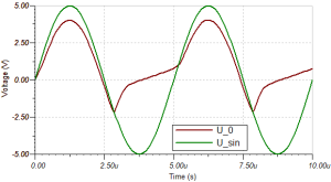
- A reverse recovery time $t_{\rm rr}$ that is too large. This is reproduced in Tina via the transit time $\rm TT$.
- an excessive junction capacity (junction capacity $C_\rm j$ or diode capacity $C_\rm D$).
- These values can be changed in Tina TI by the following procedure: Double-click on the diode » click on
…at Type » search for the mentioned values.
You now want to analyze how the reverse bias and the junction capacitance affect the voltage curve (for circuit 4).
Simulate and describe the voltage curve if- on the one hand, the reverse bias is reset to $0~\rm s$ or
- on the other hand, the junction capacitance is reset to $0~\rm F$.
describe the voltage waveform.
- Instead of diode $D=\rm 1N5400$, choose diode $D=\rm 1N4148$ and simulate again circuit 3 and circuit 1.
Now how does the voltage waveform behave and why?

Exercise 2.1.2 Calculating a series resistor for a diode
You want to drive a red light-emitting diode with a voltage source of $U_{\rm s} = 5.0 ~\rm V$ and a current of $I_{\rm D} = 20 ~\rm mA$. You have found for red LEDs a voltage drop of $U_{\rm D} = 2.3 ~\rm V$ based on a web search. Now you want to know which resistor value from the E12 series (available to you) is correct as a shunt resistor.
- Draw the circuit of the LED with a series resistor and plot the voltages.
- What is the value of the series resistor $R_\rm V$ to get the given voltage drop $U_\rm S$?
- Find the relationship between forward voltage and forward current in the datasheet of the red LED TLUR6400. What voltage drop $U_\rm D$ can be determined from this datasheet for $I_{\rm D} = 20 ~\rm mA$ and what is the correct series resistance?
- Briefly compare the different results considering the E12 series.
Exercise 2.1.3 Z-diode as voltage reference
The following circuit depicts a simple voltage reference circuit. There, a Z-diode provides a constant output voltage $U_\rm L$ on the load - despite a fluctuating input voltage $U_\rm S$ from the source.
The following quantities shall to be used:
- Source voltage $U_{\rm S}=7.0 ... 13.0~\rm V$ (e.g. via sinusoidal input voltage with $f = 50 ~\rm Hz$),
- series resistor $R_{\rm V}=1.0~\rm k\Omega $
- load resistor $R_{\rm L}= 10~\rm k\Omega $
- Z-diode $D_\rm Z$ as $\rm BZX84C6V2$ ($U_\rm Z = 6.2 ~\rm V$)

An ideal Z-diode would be assumed to hold the breakdown voltage $U_\rm Z$ at all reverse currents $I_\rm S$.
This is to be checked for the real diode.
- Model the circuit in Tina TI and insert a picture of the circuit.
- Compare the progression of $U_\rm L$ to $U_\rm S$. In particular, measure the maximum and minimum values of $U_\rm L$.
- Change the load resistance to $R_\rm L=1.0~\rm k\Omega $ and perform the same comparison of $U_\rm L$ to $U_\rm S$ again.
- How can the difference be explained?
Exercise 2.1.4 Calculating the differential resistance of a diode

The differential resistance $r_\rm D$ of a diode was already described in the chapter. This is necessary if a diode is to be simulated via a simplified diode model (voltage source + resistor + ideal diode, if applicable). In Abbildung 16, see the differential conductance $g_{\rm D}={{1}\over{r_\rm D}}$ as the local slope at the desired operating point. Calculate the differential resistance $r_\rm D$ at forward current $I_\rm D=15 ~\rm mA$ for room temperature ($T=293~\rm K$) and $m=1$ from Shockley's equation: ${I_{\rm F} = I_{\rm S}(T)\cdot ({\rm e}^{\frac{U_\rm F}{m\cdot U_\rm T}}-1)}$ with $U_{\rm T} = \frac{k_{\rm B} \cdot T}{q}$ with $q=1~\rm e$. To do this, first, calculate the general formula for the differential resistance $r_\rm D$.
Steps:
- First, simplify Shockley's equation for $U_{\rm F} \gg U_\rm T$
- Find a formula for $\frac {{\rm d} I_{\rm F}}{{\rm d} U_\rm F}$.
- Again, replace part of the result with $I_\rm F$ and rotate the fraction to calculate the differential resistance by $r_{\rm D} = \frac {{\rm d} U_\rm F}{{\rm d} I_\rm F}$.
As a result, you should now have $r_{\rm D} = \frac {{\rm d} U_\rm F}{{\rm d} I_\rm F} = \frac {m \cdot U_\rm T}{I_\rm F} $ - Calculate $r_\rm D$.
Exercise 2.1.5 Two LEDs on one digital output
For a circuit, you need to control two LEDs, but unfortunately, only one digital output is free. The supply voltage of the microcontroller and the board is $5~\rm V$. LED1 should have a forward voltage $U_{\rm F,1}=2.3~\rm V$ (red), LED2 should have a forward voltage $U_{\rm F,2}=2.1~\rm V$ (green).
- Design a circuit from the existing voltage levels so that both LEDs can be driven.
Existing voltage levels:- Supply: $5~\rm V$
- Digital output: $5~\rm V$, $0~\rm V$ or high impedance
- Calculate the values for the other necessary components
\ \ \ \ \ \ \ \ \ \ \ \.
Exercise 2.1.6 Circuit with multiple diodes
The following simulation includes multiple diodes. The shown lambs light bright, when a voltage of $5~\rm V$ or more drops over them.
Which lambs will light up, when the switch is closed?
Exercise 2.1.7 Circuit with multiple diodes II
The following simulation includes multiple diodes. Assume a simple diode model (the forward voltage drop is $V_F=0.7~\rm V$ and constant). The source voltage shall be $U0 = 4~\rm V$.
Calculate the currents through $D1$, $R1$, and $R2$.
Exercise 2.1.8 Circuit with multiple diodes III
The following simulation includes multiple diodes. Assume a simple diode model (the forward voltage drop is $V_{\rm F} = 0.7~\rm V$ and constant). The source voltage shall be $U0 = 5~\rm V$.
Calculate the currents through $R1$, $D1$, and $D2$ depending on the switch state S.
Study Questions
For self-study
- On a U-I diagram, draw the characteristic of an ideal diode and a real silicon diode and explain the differences.
- What is meant by N-doped and P-doped?
- How does a junction form inside the diode?
- What is meant by a threshold voltage?
- Why does the voltage drop across a diode?
- Sketch the layered structure of a diode and label the three layers formed.
- What kind of free charge carriers are available in each of these layers?
- Draw the electric fields formed in the diode when no external field is applied.
- Explain how an external voltage can bring the diode into a conducting state.
- Explain the working of a diode with the help of a sketch. Draw the following areas: P-doped part, N-doped part, and junction.
- Given is a layered structure of a diode (N-doping and P-doping can be seen). How would the diode have to be connected to pass current?
- Typical diode characteristic for silicon diodes.
- Draw a characteristic curve for silicon diodes.
- What is the characteristic voltage? (Technical term of voltage, the magnitude of voltage, and the relevant current range).
- Insert the technical terms for the three relevant voltage ranges.
- Z-diode
- Explain the operating principle of a Z-diode using its characteristic curve.
- Draw the current waveform of a 6V8 diode on a voltage-current diagram.
- What needs to be considered while choosing a type of diode?
- State three applications of diodes and sketch the construction.
- Rectifier circuits
- Draw a half-wave rectifier. Draw a bridge rectifier.
- Given a sinusoidal input voltage of $3~\rm V$. Draw the waveform of the input voltage and the output voltage of the two rectifiers over 2 periods for $50~\rm Hz$ in a graph.
- How can the output voltage be smoothed? How can the output current be smoothed?
- Given a sinusoidal input voltage of $3~\rm V$. What should be considered if very high frequencies are to be rectified? Draw a possible signal waveform of the input voltage and the output voltage of the two rectifiers over 2 periods for $50 ~\rm GHz$ in a diagram.
- Draw a circuit with which the positive half-wave of a sinusoidal voltage can be cut off.
with answers
Only necessary to eliminate the score bar…
Exercise - Quiz
Exercise - Quiz
Exercise - Quiz
Exercise - Quiz
Exercise - Quiz
Exercise - Quiz
- References to the media used
-
Element License Link Video: Circuit Elements - Diodes and Transistors - Part 1 CC-BY (Youtube) https://www.youtube.com/watch?v=YB3pQ7P8SNg Video: Circuit Elements - Diodes and Transistors - Part 2 CC-BY (Youtube) https://www.youtube.com/watch?v=HdXaTn-JRCo Abbildung 1 https://creativecommons.org/licenses/by-sa/3.0/de/ https://commons.wikimedia.org/wiki/File:Schema_-_n-dotiertes_Silicium.svg Abbildung 7 CC-BY-SA 3.0 https://commons.wikimedia.org/wiki/File:Schema_-_n-dotiertes_Silicium.svg Abbildung 2 https://creativecommons.org/licenses/by-sa/3.0/de/ https://de.wikipedia.org/wiki/Datei:Schema_-_p-dotiertes_Silicium.svg