This is an old revision of the document!
1. Boolean Algebra
1.0 Motivation: Digital electronics in daily life
Goals
After this lesson you should:
- know the Boolean functions, their notations, and truth tables.
- be able to apply the Boolean rules of arithmetic.
- be able to simplify Boolean expressions.
- know the following terms: (logic) gates, names of arithmetic rules.
1.0.1 Everything is one exept zero...
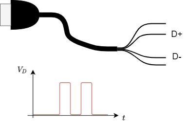
Before we start to dive deeper into the digital systems, it is a good idea to approach the topic with a first practical example. For this, we have a look onto an USB cable and mentally cut the cable. We will see a total of four wires waiting for us. Two of them are called D+ and D-. These are the wires that are used for digital data transmission. With special tools - like an oscilloscope we can measure the time course of the voltage between D+ and D-. This voltage is shows two different levels and rises and falls in between. What we see are the logic states 0 or 1!
Beyond data transmission, we can also encode other things with binary numbers: for example, we could look at
- the position of a lever - whether it is pointing up or down.
- or a switch that is open or closed.
- or a light that is on or off.
- even whether it is raining or not raining, whether a dog is barking or not barking or other things - we can encode all of that in binary units.
In reality, the measured voltage on the USB cable would also show noise and only roughly depict the two states. When we ignore the noise and only assume that an upper level (HIGH or H) encode one state and the lower one (LOW or L) the second state the diagram ist also called the level diagram. In contrast to analog systems, a signal can only take one of the two valid states in digital systems. Similarly, boolean algebra only uses the states TRUE and FALSE.
Note!
- The smallest binary message set is called a “bit”, which comes from the English term “binary digit”. A bit thus describes the logical state of a two-valued system. The binary characters can be written as, e.g.:
- '0', '1'
- FALSE, TRUE
- HIGH, LOW
- In binary logic, every expression can only be true or false. If something is not true, it has to be false - and vice versa.
- Therefore, binary logic has some limitations for real world applications: It may only rain softly, a light might be dimmed and also the voltage (which represents the bit) might be in an in-between state. This situation has to be coped with beyond the binary logic. Beyond binary logic, there is often an invalid state in reality, which separates the logic states.
We will find out more of the details behind this states in the chapter Number Systems. In this chapter we will start to think about, how this binary signals in connection with some algebra can generate a base for fundamental logic building blocks. This building blocks will be stacked together to larger boxes in the next chapters and are the basis for microcontroller, microprocessors and virtually all digital electronics from watches over automotive controllers to super computers.
 Fig. 2: Inner 'Life' of an Integrated Cicuit
1.0.2 At the heart of a computer
 Fig. 3: A 'topless' microcontroller
The core of a computer is the processor in which the instructions are executed. This central processing unit (CPU) is also used in microcontrollers, which can be found around us in almost every device: Mobile phones, cars, bank cards, washing machines… Often there are even several microcontrollers installed in the devices.
In the microcontroller, in addition to the command-executing microprocessor (more precisely, the {wp>arithmetic-logic unit}), other peripherals such as memory, clock generation, analog-to-digital converter and much more are built in. This makes it a compact tool for many applications. If you look at the microcontroller under an optical microscope, you will see the following picture (figure 3).


But now let's take a look at the structure of the processor. The processor shown in figure 4 uad figure 5 was developed by two students in 1990 and consists of several tens of thousands of transistors. This chip paved the way to cheap, fast and yet easily programmable controllers, from the fax machine to the hobby basement, and can be found on the Arduino boards, among others. You will get to know and to program the ATmega328 - a distant successor with several hundred thousand transistors - in higher semesters. The images depict various peripheral components: The processor, FLASH, EEPROM and fuses will be shown in the following chapters. The voltage supply (German 'Spannungsversorung'), is needed to generate additional higher voltages based on the supplied external voltage.
The following clip shows a zoom into the smallest parts of the controller.
One question is still unclear: how can we connect the zeros and ones in such a way, that the processor can calculate something like $23 + 42$? For this we need to have a look onto binary logic.
1.2 Binary Logic
Goals
After this lesson you should:
- know the Boolean functions, their notations, and truth tables.
- be able to apply the Boolean rules of arithmetic.
- be able to simplify Boolean expressions.
- know the following terms: (logic) gates, names of arithmetic rules.
1.2.1 First steps into logic
We have already learned about the 'bit', and it's two-valued value. This can be connected to the ancient idea of a binary logic. The Greek Philosopher Aristotle started to build up a systematic in order to conclude from statements like 'at night, it is dark outside' and 'it is night' to 'it has to be dark outside'. It might seem a bit unrelated to comtrollers and computers, at the first sight. But in this scientific interpretation of logic all logic statements are either true or false.
George Boole developed a more mathematical way into handline logic. Based on his work the fundamental logic was solidified into axioms. One axiom we have already seen: If something is true, it cannot be false ans vice versa (the 'theorem of contradiction').
Other axioms help to combine statements. This is called 'reasoning' or 'deduction'.
- This was already used some sentences before: If 'at night, it is dark outside' and 'it is night' is true, one can make the implication 'it has to be dark outside'.
But be aware, that is is not always reversible: It could also be a solar eclipse. - Another deduction is the equivalence: when 'A' implies 'B', and 'B' implies 'A' both statements are equivalent.
In the following, we will have a look onto the basic logic combinations, which are needed for digital systems. These basic logic combinations of logic statements (or bits) are called logic operators and can be used similarly to the algebraic “plus” or “minus”. The mathematical construct, which describes the systematic of these combinations is called boolean algebra. In digital systems the logic operators can be represented as a circuit of transistors or switches. This can be blackboxed into logic gates.
This tools will get more familiar in the next subcapter.
1.2.2 The logic operator NOT
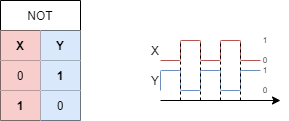
The first very simple circuit negates the input value. It is also called an inverter or negation (logic NOT, NOT gate). This logic operator always generates the output value $Y(0)=1$ from the digital input value $X=0$ and for $X=1$ correspondingly $Y(1)=0$. figure 6 shows an example: The light is only on ($X=1$), when the input is off ($Y=0$) - this functionality is “hard-wired”.
When you think about the inputs and outputs in the shown picture above, you realise, that the input is a voltage, but the output is a current. This is sometimes beneficial, but inside an digital systems commonly only voltages are used.
In order to control a (output) voltage with a (input) voltage two complement types of switches are combined similar to a voltage divider or a half bridge (see figure 7). One is normally open and the other one normally closed. This can also set up with complement types of transistors. Thus, only one transistor (TRANSfer ResISTOR) becomes conductive at a time, the other one correspondingly high impedance.
With this setup the logic voltages ($0V$, $5V$) are just switched complementary via the switches. This technique is also called CMOS technique: Complementary MOSFET. In today's electronics, this technology is used throughout and has completely replaced older variants (e.g. TTL).
Comparing the circuits in figure 6 and figure 7, one could simply see, that double the amount of switches have to be used and the lower one is a bit trickier to understand. With this in mind, for the following operators only the first type of circuit will be shown.
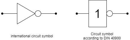
The circuit symbols of the NOT-gate are shown in figure 8. Depending on the (software) tools and schematics one of the type is printed.
Besides the symbol other representation are also common (see also figure 9):
- The truth table shows the input(s) $X$ on the left and the output(s) $Y$ on the right. There is a row for each distinct combination of inputs. This representation will get handy in the next chapters, in order to analyse more complex logic.
- The timing diagram shows the sequential behavior. For this diagram, the input variables are stimulated with all possible state combinations. Also this will become handy especialy in the chapter Sequential Logic.
- In math the inversion has also multiple representations e.g.
- $Y = /X$ (used e.g. for input with a keyboard)
- $Y = \overline{X}$ (often used when handwriting and math)
Y = !X(used in c language)
Note!
- Inputs are always denoted with $X$
- Outputs are always denoted with $Y$
- There are multiple ways for representing the logic. The most common ones are:
electric ciruit with switches (or transistors), logic gate, truth table, timing diagram, mathematical representation. - When you use a representation: use it uniformly.
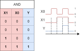
1.2.3 The logic operator AND
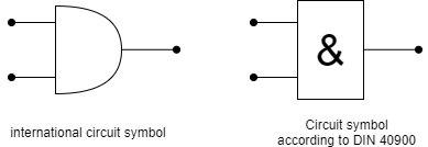
The next circuit will generate an positive output only, if all inputs are true. This is called a logical conjunction (logic AND, AND gate). When one ore more inputs are false the output is also false. figure 10 shows an example: The light is only on ($Y=1$), when all inputs are on ($X0=1$, $X1=1$, …). This is commonly used for safety circuits, e.g. when the workspace of a robot has multiple doors and all have to be closed in order to start.
Again, the other representation are shown:
- The truth table and timing diagram are depicted in figure 12.
- In math the AND operation has again multiple representations e.g.
- $Y = X0 * X1$ (used e.g. for input with a keyboard)
- $Y = X_0 \cdot X_1$ (often used when handwriting or in math)
Y = X0 && X1(used in c language),Y = X0 & X1(used in some other languages)- $Y = X_0 \land X_1$ (used in logic)
For upcoming, more complex terms the algebraic notation ($Y = X_0 \cdot X_1$) usually lead to a better understanding.
1.2.4 The logic operator NAND
The NOT gate is often used in front of or after other gates. When used after AND gates, this creates an 'NOT AND' or in short 'NAND' (logic NAND, NAND gate). This circuit will only generate an negative output only, if all inputs are true. When one ore more inputs are false the output is true. figure 13 shows an example: The light is only off ($Y=0$), when all inputs are high ($X0=1$, $X1=1$, …). In the simulation one has to look in detail: the used switches are normally closed (closed when the input is low). Therefore the switches are only open, when the input is high.
The circuit symbols are shown in figure 14. In order to shorten the ciruit, the NOT is often 'shrinked' only to a small circle after the gate.
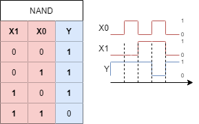
Again, the other representation are shown:
- The truth table and timing diagram are depicted in figure 15.
- In math the NAND operation has again multiple representations e.g.
- $Y = /(X0 * X1)$ (used e.g. for input with a keyboard)
- $Y = /(X_0 \cdot X_1)$ or $Y = \overline{X_0 \cdot X_1}$ (often used when handwriting or in math)
Y = !(X0 && X1)(used in c language)- $Y = /(X_0 \land X_1)$ or $Y = \overline{X_0 \land X_1}$ (used in logic)
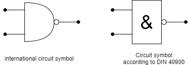
1.2.5 The logic operator OR
We already had a look onto the AND gate. So what about OR? Of course there is also this kind of operation. This is called a logical disjunction (logic OR, OR gate). When there is one or more input true the output is also true. figure 16 shows an example: The light is only off ($Y=0$), when all inputs are on ($X0=1$, $X1=1$, …). Doesn't it - at the first glimpe - seem similar to the NAND circuit? The main difference is that normally open switches are used. Only, when both switches are open the light is off.
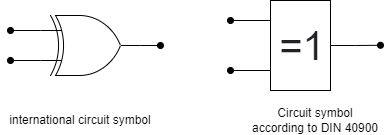
The circuit symbols are shown in figure 17. The DIN symbol is derived from the fact, that one ore more inputs have to be true to get an true output.
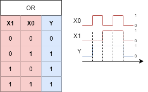
Again, the other representation are shown:
- The truth table and timing diagram are depicted in figure 18.
- In math the OR operation has again multiple representations e.g.
- $Y = X0 + X1$ (used e.g. for input with a keyboard or in handwriting)
Y = X0 || X1(used in c language)- $Y = X_0 \lor X_1$ (used in logic, the $\lor$ stands for the Latin vel, which means or)
For upcoming, more complex terms the algebraic notation ($Y = X_0 + X_1$) usually lead to a better understanding. Also here: we will see the connection to math in the next chapters.
1.2.6 The logic operator XOR
Beside the OR there is also an “either … or …, but not both”. This is called exclusive or, in short XOR (logic XOR, XOR gate). Only when one input is true the output is true. figure 16 shows an example: When none or when all inputs are on, the light is only off. The circuit looks a bit more complicated with two series branches in parallel and the use of both normally closed and normally open switches. On the other hand one can already think about, that one of the branches look similar to the setup for the AND gate, and the parallel setup similar to the NAND gate. Could it be possible to convert the gates into each other? We will see that next…
The circuit symbols are shown in figure 20. Both symbols have similarities with the OR symbols.
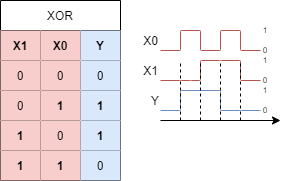
Again, the other representation are shown:
- The truth table and timing diagram are depicted in figure 21.
- In math the XOR operation has again multiple representations e.g.
- $Y = X0 \# X1$ (used e.g. for input with a keyboard or in handwriting)
- there is no bit operation in c language for XOR
- $Y = X_0 ⊕ X_1$ (used in logic)
Excercise 1.2.1. NOR and XNOR
- Think about a circuit (with multiple switches and one lamp) to implement NOR and XNOR.
- What is the relation between the circuits of NOR and AND? And how about XOR and XNOR?
- What would the gate representation and the other representations look like?
1.2.7 The Tri-State Gate
The tri-state gate is not a boolean gate, however it is still often used in logic circuits such as microcontrollers. The essence of the tri-state gate is - in short - to be able to output 'nothing'. Nothing means: neither high nor low.
One possible output of the tri-state gate - besides high and low - is 'high ohmic', which is often reffered as $Z$. In this case, the gate output is not controlled by the tri-state gate, but floats. The output can instead be controlled by an other external source. The main use of this gate is to disconnect one logic circuit from another one.
figure 16 shows the function of a tri-state gate: When the $EN$able input is set to high this gate becomes transparent and the output $Y$ equals the input $Y$. When $EN$ is set to low, the output is not pinned to the input anymore. In the simulation above with $EN = 0$ the output voltage is clamped by the voltage behind the resistor (here $3V$). Since this voltage could be any value this output cannot called low or high, but is called the (undefined) state $Z$.

The circuit symbol is shown in figure 23. Usually the triangle sybmol ist used, the DIN / EN symbol is much less common and therefore hiere ignored.
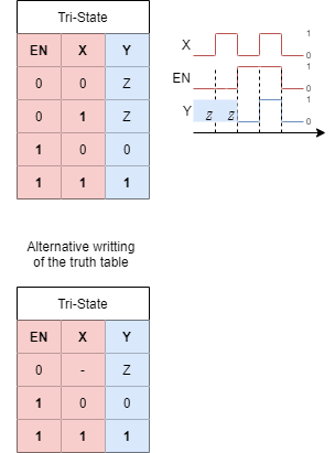
Since the Tri-State gate is not an logical gate is does not have any mathematical representation.
1.3 Convertibility of gates
Goals
After this lesson you should:
Some of the circuits in the provious chapter looked suspiciously similar. We will now have a more deeper look onto this and try to converte some gates into each other. In this subchapter we will focus on combining NAND gates in order to build other gates. As we will see, based on the NAND and NOR gates any other gate and any other logic can be created.
1.3.1 NAND in NOT
The conversion from NAND to NOT is relatively simple: When both inputs to NAND are the same (either '1' or '0') the output will be the negation of the input. This can also be seen in the truth table of the NAND gate: when the inputs as the same only the first and last row, have to be considered and lead to a inverting behaviour.
A different approach to get an NOT is to set the second input to '1'. Here, the NOT can be 'deactivated' of with the second input. This can be tested in the figure 29 by clicking on the input 'H' of the NAND gate on the right below.
1.3.2 NAND in AND
With the knwoledge from 'NAND to NOT' the NAND can be converted to AND: a negated NAND leads to an AND. It is roughly similar to 'not a no-go' is logically a 'go'. Therefore, the NOT hat to be set behind the NAND.
1.3.2 NAND in OR
When each input of a NAND gate is inverted the result acts like an OR gate. In order to understand this, one can again look onto the truth table of the NAND and the OR gate and try to invetigate what happens when the inputs of the NAND are negated.
Excercise 1.3.1. further conversions
1.4 Rules for boolean algebra
Goals
After this lesson you should:
- Understand the purpose of the Tri-State gate and the “Z” state.
- Understand the use of the “Don't care” state.
- Be able to convert interconnections from a few logic gates to truth tables and vice versa.
- Be able to trace gates to NAND and NOR gates.
We have seen, that (at least) some of the gates can be represented by means of others. In order to approach this more systematically, we will now have a look onto the arithmetic rules of boolean algebra. These rules can be used to either build a logic cicruit out of the basis gates shown in chapter 1.2. On the other hand we are also able to simplify the logic circuits by ths rules.
1.4.1 The set of rules
The following table shows the main rules which help us to generate and optimize logic expressions and circuits.
It is possible to click on “math representation” and “algebraic representation” to switch both.
Have a look for the algebraic representation. These are probably much simpler to remember!
Be also aware, that the logical expressions sometimes are written as $X0$, $X1$, … and sometimes with other letters, like $a$, $b$, …
math representation
| Nr | Math Term / Formula | Description |
|---|---|---|
| 1 | Closure | The operators $\land$ and $\lor$ map elements from $B=\{a,b,...,n\}$ to $B$. |
| $B \land B \rightarrow B $ | ||
| $B \lor B \rightarrow B $ | ||
| 2 | Duality | If $A$ is a statement of boolean algebra, so is $A^*$. $A^*$ is obtained by exchanging $\land$ with $\lor$ and vice versa. |
| 3 | Neutral Element | There exist a neutral element to the operators $\land$ and $\lor$. Applying the oparator to a and the neutral element results in $a$. |
| $a \land 1 = a $ | ||
| $a \lor 0 = a $ | ||
| 4 | Complementary Element | There exist a complementary element to the operators $\land$ and $\lor$. The negation of $a$ is for both operators the complementary element. |
| $a \land \bar{a} = 0 $ | ||
| $a \lor \bar{a} = 1 $ | ||
| 5 | Idempotence | Applying the operators $\land$ and $\lor$ to a similar input a results in $a$. |
| $a \land a = a $ | ||
| $a \lor a = a $ | ||
| 6 | Commutative Law | Inputs $a$ and $b$ are interchangable. |
| $a \land b = b \land a $ | ||
| $a \lor b = b \lor a $ | ||
| 7 | Associative Law | For the same operator bracketing can be moved. associative means “to unite” or “to connect” |
| $a \land (b \land c) = (a \land b) \land c $ | ||
| $a \lor (b \lor c) = (a \lor b) \lor c $ | ||
| 8 | Distributive Law | The bracketing is similear like for multiplication: $a \cdot (b + c) = (a \cdot b) + ( a \cdot c) $. However this is true for both boolean operators! |
| $a \land (b \lor c) = (a \land b) \lor (a \land c)$ | ||
| $a \lor (b \land c) = (a \lor b) \land (a \lor c)$ | ||
| 9 | Law of Absorbtion | In bracketed formulas similar expressions can “absorb” each other. This law can be drived from the laws (8), (5), (7) |
| $a \land (a \lor b) = a$ $a \land (\bar{a} \lor b) = a \land b $ |
||
| $a \lor (a \land b) = a$ $a \lor (\bar{a} \land b) = a \lor b $ |
||
| 10 | DeMorgan's Rule | $\land$ can be written as $\lor$, BUT one has to negate the inputs and outputs |
| $\overline{a\land b} = \overline{\overline{\bar{a}\lor \bar{b}}} = \bar{a}\lor \bar{b} $ $ \bar{a}\lor \bar{b}= \overline{\bar{\bar{a}}\land \bar{\bar{b}}} = \overline{a\land b} $ |
||
| $\overline{a\lor b} = \overline{\overline{\bar{a}\land \bar{b}}} = \bar{a}\land \bar{b} $ $ \bar{a}\land \bar{b}= \overline{\bar{\bar{a}}\lor \bar{\bar{b}}} = \overline{a\lor b} $ |
algebraic representation
| Nr | Math Term / Formula | Description |
|---|---|---|
| 1 | Closure | The operators $\cdot$ and $+$ map elements from $B=\{a,b,...,n\}$ to $B$. |
| $B \cdot B \rightarrow B $ | ||
| $B + B \rightarrow B $ | ||
| 2 | Duality | If $A$ is a statement of boolean algebra, so is $A^*$. $A^*$ is obtained by exchanging $\cdot$ with $+$ and vice versa. |
| 3 | Neutral Element | There exist a neutral element to the operators $\cdot$ and $+$. Applying the oparator to a and the neutral element results in $a$. |
| $a \cdot 1 = a $ | ||
| $a + 0 = a $ | ||
| 4 | Complementary Element | There exist a complementary element to the operators $\cdot$ and $+$. The negation of $a$ is for both operators the complementary element. |
| $a \cdot \bar{a} = 0 $ | ||
| $a + \bar{a} = 1 $ | ||
| 5 | Idempotence | Applying the operators $\cdot$ and $+$ to a similar input a results in $a$. |
| $a \cdot a = a $ | ||
| $a + a = a $ | ||
| 6 | Commutative Law | Inputs $a$ and $b$ are interchangable. |
| $a \cdot b = b \cdot a $ | ||
| $a + b = b + a $ | ||
| 7 | Associative Law | For the same operator bracketing can be moved. associative means “to unite” or “to connect” |
| $a \cdot (b \cdot c) = (a \cdot b) \cdot c $ | ||
| $a + (b + c) = (a + b) + c $ | ||
| 8 | Distributive Law | The bracketing is similear like for multiplication: $a \cdot (b + c) = (a \cdot b) + ( a \cdot c) $. However this is true for both boolean operators! |
| $a \cdot (b + c) = (a \cdot b) + (a \cdot c)$ | ||
| $a + (b \cdot c) = (a + b) \cdot (a + c)$ | ||
| 9 | Law of Absorbtion | In bracketed formulas similar expressions can “absorb” each other. This law can be drived from the laws (8), (5), (7) |
| $a \cdot (a + b) = a$ $a \cdot (\bar{a} + b) = a \cdot b $ |
||
| $a + (a \cdot b) = a$ $a + (\bar{a} \cdot b) = a + b $ |
||
| 10 | DeMorgan's Rule | $\cdot$ can be written as $+$, BUT one has to negate the inputs and outputs |
| $\overline{a\cdot b} = \overline{\overline{\bar{a}+ \bar{b}}} = \bar{a}+ \bar{b} $ $ \bar{a}+ \bar{b}= \overline{\bar{\bar{a}}\cdot \bar{\bar{b}}} = \overline{a\cdot b} $ |
||
| $\overline{a+ b} = \overline{\overline{\bar{a}\cdot \bar{b}}} = \bar{a}\cdot \bar{b} $ $ \bar{a}\cdot \bar{b}= \overline{\bar{\bar{a}}+ \bar{\bar{b}}} = \overline{a+ b} $ |
The last 3 laws are probable a kind of unintuitive. Therefore, these are shown in other representations. in the following
1.4.2 Dive into Distributive Law
The distributive law can be shown on a simple example of daily life.
When one says
"I'm happy with fries AND (a water OR a coke)"
he will be happy with
(fries AND a water) OR (fries AND a coke)
Be aware, that the is no exclusiveness here. The person would also be happy with fries AND a water AND a coke!
The gate represenation is shown in figure 32. At the first glimpse, the output $Y$ of the upper circuit and the lower circuit look similar (they are indeed the same).
Also the truth tables for the first gate ($Y'$, $Y''$, $Y'''$) and a larger truth table for all results is given.
But the conversion of the upper one to the lower one is not intuitive here. That is why the multiple represenations and remembering the rules for boolean algebra is very important. Translating from one represenation into another one helps to use other tools in order to simplify systems!
1.4.3 Dive into Law of Absorbtion
We will also try to transfer the law of absorbtion to a example of daily life.
When one says
"I'm happy with fries OR (fries AND a coke)"
he will be happy with
fries..
No matter whether there is coke with it.
The absortion of the inverse ($a + (\bar{a} \cdot b) = a + b $) is also possible:
When one says
"I'm happy with fries OR (no fries AND a coke)"
he will be happy with
fries OR a coke
When he only gets fries the first part is true. When he only gets coke, the secont part is true. When he gets both, he of cource gets fries and therefore the firt part is true..
The gate represenation is shown in figure 33. When ignoring the blinking High and Low of the lines, also here the similarity of the upper and lower circuits may be not really intuitive.
1.4.4 Dive into DeMorgan's Rule
At last, let's have a look onto DeMorgan's rule. The following instance shows it in daily life.
When one says
"I don't like fries AND i don't like coke"
he will be unhappy when he gets either fries, or coke, or (fries and coke).
The gate represenation is shown in figure 34. All four circuits show the same behaviour.
On the left the NOT gate is explicitely shown. On the right the NOT gates are shrinked down to the circles either on the input or on the output.
The important thing about DeMorgan's rules is: any expression stays the same, when
- all parts of the expression are inverted plus
- any AND is substituted with OR plus
- any OR is substituted with AND
Important is, that also the most upper expression also have to be inverted.
1.4.5 Example of a logic simplification
1.5 Examples of gate circuits
1.5.1 Logic gates with multiple inputs
Based on the associative law, when purely AND gates or purely OR gates are stacked the inputs are interchangeable.
Therefore, this stacking can be substituted with a gate symbol with multiple input. The two AND-gates shown in figure 35 can be substituted with a single one.
The essence auf the AND gate is: An AND gate - no matter how much inputs it has - will only output high, when all inputs are high.
Excercise 1.5.1. Other gates with multiple inputs
- What is the essence of an OR gate? what will the truth table of an OR gate with 3 inputs look like?
- What is the essence of an XOR gate? what will the truth table of an XOR gate with 3 inputs look like? (keep in mind, that this question might have multiple answers for XOR)
1.5.2 Switchable inverter
Sometimes it is important switch between inverting and not inverting an output. This can be done with the XOR gate. When the $EN$ in figure 36 is active, the input $X$ will be inversed.
One application for a switchable inverter would be an monochrome display, where every pixel can be set by one bit. When the display (or a small part like the cursor symbol) has to be inverted it would be great to do so with a simple gate. This can be seen in this more complex example, where the display smiley can be inverted via the XOR gate during data transmission. The other logic component in this example will be explained in the following (sub)chapters.
Another usage is the inversion of binary numbers in the arithmetic logical unit of the processor.
1.5.3 Data valve
To deactivate a data flow a simple AND gate can be used. This is also useful for channelize data in multiple directions.
In the upper part of figure 37 a single data valve is shown. Only when $EN=1$, then the value of $X$ will set as the output $Y$.
The lower part of figure 37 shows the combination of two data valves. In this circuit depending on $EN$ the output of the $X$ will either be $Y0$ or $Y1$. This is also visible in the truth table.
1.5.4 Multiplexer and Demultiplexer
In the linked 'display example' in 1.5.2 there were a Multiplexer (MUX) and a Demultiplexer (DEMUX) visible.
A multiplexer is a electronic switcher, which has several data inputs $D0$, $D1$ … and one data output $Y$. Additionally to the data input there are also state inputs $S0$, $S1$, … . The state inputs address which of the data input is routed to the data output. An example is given in figure 37. When $S0 = 0$ and $S1 = 0$ the zeroth data input $D0$ is the output, for $S0 = 1$ and $S0 = 0$ the first data input $D1$, for $S0 = 0$ and $S0 = 1$ the second. The 'inner live' of the multiplexer will be shown in the chapter 3.
A demultiplexer is the counterpart to the multiplexer: It has one data input $D$ and several data outputs $Y0$, $Y1$, … . Again there are also state inputs $S0$, $S1$ … . Here, the state inputs address to which data output the single data input is routed. also this is shown in figure 37.
1.6 Rules for boolean algebra
zwei Transistor(typ)en reichen
Ok, now we know at least that the chip consists of many transistors. But how do they work and how can you build something as complex as a processor from them? The exact function is the content of the course '(Analog) Circuit Design'. For digital applications it is sufficient to have a simple picture of a certain type of transistor - the MOSFET - in your head. This has the three terminals:
- Source (“Quelle”), the inflow of charge carriers
- Drain (“Senke”), the outflow of the charge carriers
- Gate (“Tor”), the gatekeeper, which regulates the passage between source and drain: If the correct voltage gate is present at the gate terminal 1), the Source and Drain terminals are short-circuited, that is, a current can flow and the voltage drop between them becomes small.
Two types of MOSFET are important in the following digital circuits:
- one that is non-conductive for low voltages ($0V$, logic $0$, Low, $L$, or False) at the gate (n-channel MOSFET) and
- one that is non-conductive for high voltages ($5V$, logic $1$, High, $H$ or True) at the gate (p-channel MOSFET).
In the picture on the right (figure ##) you can see the two variants in action, when the voltage at the gate just assumes the digital voltage values.
Now it is interesting, that these two kinds of transistors are sufficient to build all variants of logical functions. Logical functions combine one or more inputs ($X_1, ... X_n$) in such a way, that every kind of input uniquely leads to an output ($Y_1, ... Y_n$). In circuits, so-called gates correspond to logical functions. They need not be only such simple functions like an AND-gate. Mathematical operations can also be mapped in this way. To do this, gates must be cleverly combined with each other. In an exercise on binary logic, it is shown that all gates can be constructed using NAND or NOR gates. So, if we could figure out how to build a NAND or NOR gate from transistors, we could in turn build all gates up to addition from it.
Gatter logisch?
Before the NAND gate is considered, a very simple circuit is to build, which generates the output value $Y(0)=1$ from the digital input value $X=0$ and for $X=1$ correspondingly $Y(1)=0$. This circuit always negates the input value and is called inverter. For this purpose the two types of transistors are combined similar to a voltage divider or a half bridge. Thus, only one transistor (TRANSfer ResISTOR) becomes conductive at a time, the other one correspondingly high impedance. In figure 6 the corresponding circuit with normally open and normally closed switch is also drawn. It is important for the following consideration that the logic voltages ($0V$, $5V$) are just switched complementary via the switches. For this reason this technique is also called CMOS technique: Complementary MOSFET. In today's electronics, this technology is used throughout and has completely replaced older variants (e.g. TTL).

From this example, it can be seen how a logical $1$ can become $0$ in mobile phones, vehicle control units, and television sets. The figure 2 shows the realization of this gate in silicon:
- Figure (1) shows the image of a scanning electron microscope, which shows several layers at the same time. The three circular elements are electrical passages (“vias”) through several layers. In green are the two structures of the MOSFETs, which can act as a “valve” to open the connection up ($5V$) or down ($0V$).
- Figure (2) is a false color image. In beige is the top conductive layer and in blue is the non-conductive region of the top layer.
- In figure (3), the different signals have been highlighted.
The output $A$ is taken out via a via with the right connection.
not-AND, or?
But how does the NAND gate work, on which logic can be built it? The concept behind this gate is that the output will only output logic false ($Y=0$) if both inputs are set to logic true ($A=1$ and $B=1$). The gate is shown in figure 7 above. This must be implemented using the two types of transistors , which were already explained. So, this structure must be built in such a way that:
- only if both inputs switch transistors with $A=1$ and $B=1$ at the same time, $0V$ shall be applied,
- if one of the inputs $A$ or $B$, or both equal 0, $5V$ shall be applied.
The first one is possible via a series connection of transistors at $0V$. These must short the source and drain terminals at a gate voltage of $5V$ (input to logic $1$), so n-channel MOSFETs are required.
The second one requires a parallel connection of transistors against $5V$. These must short the source and drain with a gate voltage of $0V$. Here p-channel MOSFETs are used (figure 7 below).
The implementation in silicon (figure ##) again appears somewhat unclear at first glance. In this figure three pictures are to be seen, again. In the first picture the transistors are marked green again and also the vias are to be recognized again over white circles. If you take a closer look at the diagram, you will notice that the via at $5V$ can be reached via the left or right MOSFET. However, the via at $0V$ can only be reached if both lower MOSFETs short-circuit. Thus, the structure is consistent with the circuit determined so far. The figure ## and figure 10 should show this in more details.
")
eine einfache Rechnung
Wie können nun die NAND-Gatter so verschaltet werden, dass das Rechenwerk Operationen wie $y=a+b$ durchführen kann? Dazu wird die Operation zunächst nur für binäre Werte betrachtet. Um die binäre Größen von dezimalen Größen zu unterscheiden wird diesen ein $0b$ vorangestellt. Folgende Kombinationen sind also möglich:
- $0 + 0 = 0$ bzw. $0b0 + 0b0 = 0b00$
- $0 + 1 = 1$ bzw. $0b0 + 0b1 = 0b01$
- $1 + 0 = 1$ bzw. $0b1 + 0b0 = 0b01$
- $1 + 1 = 2$ bzw. $0b1 + 0b1 = 0b10$
Es ist zu sehen, dass nur wenn beide Eingänge gerade $1$ sind die zweite Stelle des Bitwertes gesetzt ist. Dies entspricht gerade einem AND. Da aber alles aus NAND-Gattern aufgebaut werden soll, muss eine geschickte Zusammenschaltung dieser Gatter gefunden werden. Hierzu wird einem NAND-Gatter ein Inverter-Gatter nachgeschalten. Das Inverter-Gatter wiederum erhält man über ein NAND-Gatter, wenn beide Eingänge verbunden werden. In figure 12 ist diese Schaltung unten durch die beiden unteren NAND-Gatter dargestellt.
Auch für die erste Stelle des Bitwertes lässt sich eine Schaltung finden. Wie kann man auf diese Schaltungen kommen? Dies wird im Kapitel Schaltnetze erklärt.
Werden viele Eingänge oder Ausgänge zusammengefasst, können größere Zahlenwerte umgesetzt werden. Das heißt, die Rechnung $3+3$ bzw. im binären $0b\color{green}1\color{violet}{1} + 0b\color{blue}{1}\color{red}{1}$ wird auf mehrere Einzelrechnungen heruntergebrochen. Dies ähnelt der händischen Addition durch Untereinanderschreiben der Zahlenwerte und schrittweiser Rechnung. In diesem Beispiel müsste zunächst $0b\color{violet}{1} + 0b\color{red}{1}$ berechnet werden, was $0b\boldsymbol{1}0$ ergibt. Im nächsten Schritt $0b\color{green}1 + 0b\color{blue}{1}$ muss zusätzlich noch der Überlauf aus der vorherigen Rechnung $0b\boldsymbol{1}$ berücksichtigt werden. So können prinzipiell beliebig lange Zahlen miteinander verknüpft werden.
Um die Zahlen handhabbarer für Mensch und Maschine zu gestalten wurde eine sinnvolle Gruppierung eingerichtet: 8 binäre Zahlenwerte werden zu einem Byte zusammengefasst. Dieses kann für Menschen lesbar als Dezimalwert $0...255$ oder Hexadezimalwert $0x00 ... 0xFF$ in Programmen dargestellt werden. Im Microprozessor werden diese Zahlenwerte stets als Binärwert gehandhabt.
Nano-Lego

related Links
- Solver for Boolean functions: The solver specifies with which axioms Boolean equations can be simplified.
- Wolfram Alpha shows the different representations for boolean statements
- Silicon Zoo: Here you can see the practical implementation of logic gates in silicon.
- A nice overview of core ideas for calculating with electricity has been compiled by Gymnasium Kirchenfeld (CH, in German)
- Explanation of CMOS in the english Wikipedia
- Wiki page on integrated circuits
Applications
- Etherium: With this cryptocurrency, calculations on the blockchain are possible. Here, the basic logical functions are the most convenient - so a program should be feasible with as few boolean operators as possible
- Example in C for using of boolean algebra: by clicking on the Fork this button, the code can be changed.
Excercises
Details can be found in Introduction to Digital Systems
References
- figure ##: David Carron@Wikimedia,public domain