Dies ist eine alte Version des Dokuments!
Realization of Combinatorical Logic
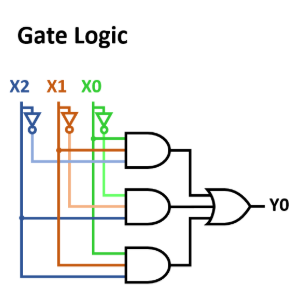
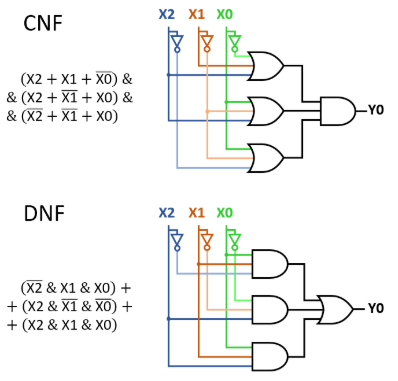
In the last chapter we investigated the Therm-o-Safety example. From this, it was possible to create the logic formula via sum of products of products of sums (see Abbildung 1).

It is simple to derive the gate logic from the formula (Abbildung 2). For each of the three (min)terms an AND-gate combines the needed inputs. As shown in the image, usually parallel to the inputs also the inverted inputs are drawn.
The main question is now: which generalization of the shown logic can be found?
History of the Logic Families
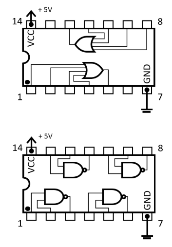
A huge variety of integrated circuits (ICs) were used historically. Abbildung 3 shows two separate integrated circuits: There can be single or multiple gates in an IC with two or more inputs. The most used IC series was the 74xx ICs, where the xx are numbers which define the internal logic.
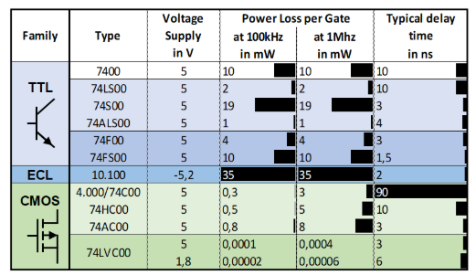
The logic families which were first developed were based on bipolar transistors. To use these as an closed switch a constant current is needed. This result in relatively high power losses. Depending on the combination of these transistors this logic families were called „transistor transistor logic“ (TTL) or „emitter coupled logic“ (ECL). The name TTL survived as a designation for the needed voltage levels $0V$ and $5V$. The $5V$ can still be found as supply voltage in some logic circuits.
Modern controller an logic is based on CMOS. Abbildung 4 shows that this type of logic only disipates a fraction of the energy loss (and therefore heat) compared to the older logic families. This started the logic circuit develompent, which lead to mobile phones, computer and all the other present digital controller.
The 74xx series is nowadays mostly from historical interest. Nearly all of the applications can now be done directly with microcontrollers. In rare cases they are still used as „glue logic“ between two logic ICs, e.g. as for adjusting the logic voltage level.
Logic Stages
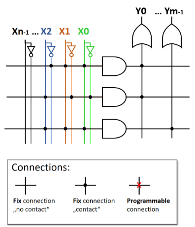
From the <img pic02> we know how the logic for the sum of products looks like. in Abbildung 5 also the gate logic for the product of sums is shown. Both consist of two logic stages:
- For sum of products the first logic stage are the OR-gates, the second stage is the AND-gate,
- For product of sums, it is just the other way around: first logic stage AND-gates, second stage OR-gate.
Generally, the two-stage setup allows to implement any possible logic based on a truth table.
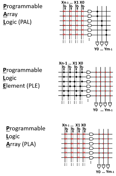
Often a simplification of the circuit represenation is used. There the multiple input ant output lines are reduced to one single line, representing a bus (= multiple parallel lines). Only the inputs which where the crossing of the lines are marked with a black dot are used as an input for the stages. These nodes are programmable and are usually set during production. The logic stages can be seen in Abbildung 6.