This is an old revision of the document!
5. Storage Elements
In the previous chapter we have had a look onto memory devices, which store data even when no voltage is applied. This is great for longterm storage, like measurement data, pictures or music. The clock frequency of the storage element are often much lower than the internal frequency of the processor / controller. By this, the processor has to wait for the stored information due to high access time.
Therefore an controller-internal memory is advantageous. These are often called cache. Distinct storage elements have special properties, e.g. the written data changes the logic level of a pin ('foot') of the IC directly. We will now focus onto these controller-internal, fast memory, which consist of logic gates.
The name flipflop stems from the fact, that the smallest logic circuit for storing data has to store binary values. Therefore, it has to show one of two stable states, and can flip into the other one by an external interaction.
5.1 Evolution of a Flipflop
Flipflop as a Blackbox
In order to understand the wanted storage element, we will first look onto these element based on the IPO model (input–process–output).
The process of the storage element is to store two different states. This property can be implemented via two inverting gates which are interconnected in a feedback loop. The simple setup would be with NOT gates as shown in figure 1.
Of course this simple elements misses inputs and outputs! Therefore we have to look into these now.
The input of this element needs at least two inputs. Often the following two are used:
- Set input: once this input is high, a $1$ is stored. This input is marked as $S$.
- Reset input: once this input is low, a $0$ is stored. This input is marked as $R$.
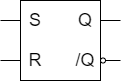
For the output also often two pins are shown. The pin $Q$ outputs the stored data directly. The pin $/Q$ outputs the inverted value.
Based on this simple requirements we can create the truth table.
- When $S=0$ and $R=0$, nothing changes and the outputs stay the same: $Q(n+1)=Q(n)$, $/Q(n+1)=/Q(n)$
- When $S=1$ and $R=0$, the stored information will be set: $Q(n+1)=1$, $/Q(n+1)=0$
- When $S=0$ and $R=1$, the stored information will be reset: $Q(n+1)=0$, $/Q(n+1)=1$
- When $S=1$ and $R=1$, it is unclear what to do.
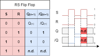
In figure 2 the last input ($S=1$, $R=1$) reaches a not defined state. This state have to be investigated more later.
RS flip flop - Open the Blackbox
First, the storage device have get some inputs in order to change the stored stage. For This, a “switchable” NOT-gate is needed. Looking back to the chapter Boolean Algebra - Convertibility of Gates, this can be achieved by NAND gates or NOR gates.
In figure 3 a first approach is shown.
But how are the inputs $X_0$ and $X_1$ related to $S$ and $R$, as well as the outputs $Q$ and $/Q$ to $Y_0$ and $Y_1$?
In this introduction, only flip flops based on NOR gates are discussed - but flip flops are can also be build up with NAND gates. In figure 4 such a NOR flip flop is shown. Compared to figure 3 the outputs had to be rearranged in order to have the pins sorted as shown in the logic symbol (see figure 5)
So let's analyze how this setup works! Therefore, the circuit in figure 4 has to be analyzed:
- Initially, $Q=0$ and the both inputs are $0$. This is due to the facts, that:
- The upper NOR gate has also two $0$s as an input a outputs consequently $/Q=1$.
- This $1$ is also an input to the lower NOR gate.
- This respectively generates $Q=0$. This situation is stable.
- When setting $S=1$ multiple things will happen successively:
- At first, the upper NOR gate has a $1$ on the input, which results into a $0$ at the output, and on $/Q$.
- With $/Q=0$ also both inputs of the lower NOR gate are $0$.
- Therefore, the lower gate generates $Q=1$.
- The stored data is also stable:
- This means $Q=1$, even when going back to the initial state $S=0$ and $R=0$.
- The upper NOR gate still has one input set to $1$ and consequently still generates a $0$.
- The only way to clear $Q$ (i.e. to set $Q=0$) is by setting $R=1$
- This this input the lower NOR gate has a $1$ as an input and outputs $Q=0$.
- By $Q=0$ the inputs of the upper NOR gate also both get $0$.
- This results in $/Q=1$
The only problem (or better inconsistency) appears, when setting both inputs to $1$:
- By this, both NOR gates generates $0$s
- This on the one hand creates $Q=1$ and $/Q=1$, which is not consistent.
This will get even more problematic:
- Both gates show typically not the exact same behaviour in respect to setting their outputs on a sub-microsecond scale to the voltage comparable with the logic $1$ or $0$.
- Therefore, once one will set the flip flop back to the initial state $S=0$ and $R=0$ both NOR gates compete to set their output to $1$. The faster one will win.
- This results in an arbitrary behavior.
D-Latch - Solving the Inconsistencies
In order to solve this undefined behavior one simple solution is to have the reset input $R$ be always the negation of $S$. This single input solution is shown in figure 6. The input name is now changed to $D$, which refers to the stored data.
However, this rises a “small problem”: now the state can be changed, but set and reset is based on one single input. Therefore, it is not a storage device, but more a kind of a delay: when the input data changes, the output changes after a constant short timespan, too.
In order to solve this next problem, another input $C$ is introduced (see figure 7). Only for $C=1$ changes in the stored states are possible: For $C=1$ the flip flop gets transparent. Once $C=0$, no changes in the state can be done.