This is an old revision of the document!
5. Storage Elements
In the previous chapter we have had a look onto memory devices, which store data even when no voltage is applied. This is great for longterm storage, like measurement data, pictures or music. The clock frequency of the storage element are often much lower than the internal frequency of the processor / controller. By this, the processor has to wait for the stored information due to high access time.
Therefore an controller-internal memory is advantageous. These are often called cache. Distinct storage elements have special properties, e.g. the written data changes the logic level of a pin ('foot') of the IC directly. We will now focus onto these controller-internal, fast memory, which consist of logic gates.
The name flip-flop stems from the fact, that the smallest logic circuit for storing data has to store binary values. Therefore, it has to show one of two stable states, and can flip into the other one by an external interaction.
A good example for the usage of complex logic circuits ca be seen in (part of) the interactive circuit for the game pong. In this circuit are - besides a lot of known gates - also some components called “counter” ans some with inputs named $D$ or $J$ and $K$. But what are these? This shall be explained in the following sub-chapters.
5.1 Evolution of a Flip-Flop
A nice, short introduction can be found in the following video:
5.1.1 Flip-Flop as a Blackbox
In order to understand the wanted storage element, we will first look onto these element based on the IPO model (input–process–output).
The process of the storage element is to store two different states. This property can be implemented via two inverting gates which are interconnected in a feedback loop. The simple setup would be with NOT gates as shown in figure 1.
Of course this simple elements misses inputs and outputs! Therefore we have to look into these now.
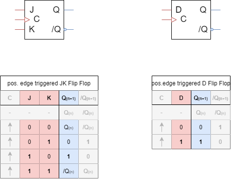
The input of this element needs at least two inputs. Often the following two are used:
- Set input: once this input is high, a $1$ is stored. This input is marked as $S$.
- Reset input: once this input is low, a $0$ is stored. This input is marked as $R$.
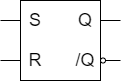
For the output also often two pins are shown. The pin $Q$ outputs the stored data directly. The pin $/Q$ outputs the inverted value.
Based on this simple requirements we can create the truth table.
- When $S=0$ and $R=0$, nothing changes and the outputs stay the same: $Q(n+1)=Q(n)$, $/Q(n+1)=/Q(n)$
- When $S=1$ and $R=0$, the stored information will be set: $Q(n+1)=1$, $/Q(n+1)=0$
- When $S=0$ and $R=1$, the stored information will be reset: $Q(n+1)=0$, $/Q(n+1)=1$
- When $S=1$ and $R=1$, it is unclear what to do.
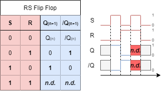
In figure 2 the last input ($S=1$, $R=1$) reaches a not defined state. This state have to be investigated more later.
5.1.2 RS Flip-Flop - Open the Blackbox
First, the storage device have get some inputs in order to change the stored stage. For This, a “switchable” NOT-gate is needed. Looking back to the chapter Boolean Algebra - Convertibility of Gates, this can be achieved by NAND gates or NOR gates.
In figure 3 a first approach is shown.
But how are the inputs $X_0$ and $X_1$ related to $S$ and $R$, as well as the outputs $Q$ and $/Q$ to $Y_0$ and $Y_1$?
In this introduction, only flip-flops based on NOR gates are discussed - but flip-flops are can also be build up with NAND gates. In figure 4 such a NOR flip-flop is shown. Compared to figure 3 the outputs had to be rearranged in order to have the pins sorted as shown in the logic symbol (see figure 5)
So let's analyze how this setup works! Therefore, the circuit in figure 4 has to be analyzed:
- Initially, $Q=0$ and the both inputs are $0$. This is due to the facts, that:
- The upper NOR gate has also two $0$s as an input a outputs consequently $/Q=1$.
- This $1$ is also an input to the lower NOR gate.
- This respectively generates $Q=0$. This situation is stable.
- When setting $S=1$ multiple things will happen successively:
- At first, the upper NOR gate has a $1$ on the input, which results into a $0$ at the output, and on $/Q$.
- With $/Q=0$ also both inputs of the lower NOR gate are $0$.
- Therefore, the lower gate generates $Q=1$.
- The stored data is also stable:
- This means $Q=1$, even when going back to the initial state $S=0$ and $R=0$.
- The upper NOR gate still has one input set to $1$ and consequently still generates a $0$.
- The only way to clear $Q$ (i.e. to set $Q=0$) is by setting $R=1$
- This this input the lower NOR gate has a $1$ as an input and outputs $Q=0$.
- By $Q=0$ the inputs of the upper NOR gate also both get $0$.
- This results in $/Q=1$
The only problem (or better inconsistency) appears, when setting both inputs to $1$:
- By this, both NOR gates generates $0$s
- This on the one hand creates $Q=1$ and $/Q=1$, which is not consistent.
This will get even more problematic:
- Both gates show typically not the exact same behaviour in respect to setting their outputs on a sub-microsecond scale to the voltage comparable with the logic $1$ or $0$.
- Therefore, once one will set the flip-flop back to the initial state $S=0$ and $R=0$ both NOR gates compete to set their output to $1$. The faster one will win.
- This results in an arbitrary behavior.
5.1.3 D-Latch - Solving the Inconsistencies
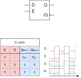
In order to solve this undefined behavior one simple solution is to have the reset input $R$ be always the negation of $S$ 1). The input name is now changed to $D$, which refers to the stored data.
This single input solution is shown in figure 6. The upper ciruit in figure 6 shows a common problem: when the ciruict is not prepared correctly, the output could show an intermediate inconsistent situation. This can be seen for the switch from $D=0$ to $D=1$. For a short time the outputs are $Q=/Q=0$. A solution is to use a buffer (symbol “▷”). A buffer delays the signal for a similar timespan like a NOT-gate, but without negating the signal (shown in figure 6 below).
However, this circuit rises a “small problem”: now the state can be changed, but set and reset is based on one single input. Therefore, it is not a storage device, but more a kind of a delay: when the input data changes, the output changes after a constant short timespan, too.
In order to solve this next problem, another input $E$ for enable is introduced (see figure 7). Only for $E=1$ changes in the stored states are possible: For $E=1$ the circuit gets transparent. Once $E=0$, no changes in the state can be done.
The given circuitry is also called D-Latch with the symbol shown in figure 8.
Generally, the term latch is used, when there is a transparent time span. Otherwise the circuit is called flip-flop.
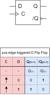
5.1.4 Edge-Triggered D Flip-Flop - One at a time
In digital systems the data processing is done clocked (i.e. once in a cycle). In the sub-chapter before, the input $C$ was introduced. Once this input changes to $C=0$, the data could be used in the next logic stage.
Digital systems often need to be power efficient, in order to save energy and avoid overheating. A disadvantage of the D-latch is, that in the transparent phase, the signal can change often until it gets stored at the end of the phase. For every transistion, a small additional current flow is needed. Therefore, the D-latch is not as power efficient, and would also pass on the transistions to the next logic stages.
In order to change the full transparency into a single change per cycle, a circuit based on two D-latches in series can be used. In figure 9 the two latches can be seen in the upper part. The first latch is enabled with the negated clock input $C$. Therefore, the first latch is only transparent for $C=0$. The second latch gets the double negated clock input, which means, it is only transparent for $C=1$. The output is changed (and $D$ is stored only for the switch from $C=0$ to $C=1$. By this, the state of $D$ is only stored, when switching $C$. When the switch from $C=0$ to $C=1$ is used, then this point in time is called positive edge.
The lower part in figure 9 and figure 10 shows the symbol of the D flip-flop.
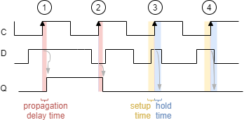
There are some important timing issues of all the flip-flops and latches, which will discussed here. For this, the timing diagram of a positive edge triggered D flip-flop is shown in figure 11. The upper line depicts the clock $C$, the middle line dhe data $D$ and the lower one the output $Q$.
- The first positive edge, shows a delay between the triggering edge on $C$ and a resulting change in $Q$. This is called the propagation delay time $t_{PD}$. This delay reflects the time for the flip-flop to “process” the data.
- At the second positive edge the data line $D$ is long enough low in order to switch the state of the flip-flop to $0$
- At the third edge, the setup time $t_{su}$ and the hold time $t_h$ is shown. When the change of the data input $D$ is not long enough the state of the flip-flop is likely not to be changed. The data on the third edge starts too late to be high. Therefore, the output $Q$ stays $0$
- On rhe last edge the data input is not long enough at high to change the internal state of the flip-flop.
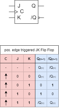
5.1.5 JK Flip-Flop - The Alternative to the undefined Behavior
The D flip-flop was generated based on a circuit with a series connection of two latches. Another idea could be to try a similar logic cicruit based on two RS flip-flops. This can be seen in figure 12. It looks like a valid storage device: with $R=1$ and $S=0$ a rising edge clears the stored bit $Q=0$. Respectively, with $R=0$ and $S=1$ the stored bit is set and the output is $Q=1$. However, $S=1$ and $R=1$ still creates an undefined behavior.
A nice tweak is to feedback the outputs $Q$ and $/Q$ to the input AND-gate (see figure 13). This prohibits the undefined behaviour. At the beginning the output $Q$ and $/Q$ is set correctly on the rightside RS flip-flop. Therefore, the feedback of $Q$ and $/Q$ only enables one AND-gate. With this start the undefined states cannot be reached anymore. The input $R=1$ and $S=1$ creates instead a toggling output for each edge on the clock $C$. This can also be seen in the truth table in figure 14.
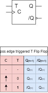
5.1.6 T Flip-Flop - changeable, when wanted
For the JK flip-flop one input value toggles the output. This can also be used to creat a nuew type of flipflop. For this the $J$ and $K$ inputs are combined to a $T$ (=toggle) input. This can also be seen in the truth table in figure 16.
5.2 Convertibility of Flip-Flops
The precious chapter showed different flip-flops - but which are important to understand and remember? Mainly, this are:
- the asynchronous RS flip-flop as a base of all the other flip--flops and its use in ICs like the timer 555
- the edge triggered D flip-flop as a simple storage device of one bit.
- the edge triggered T flip-flop as one building block for counter and other sequential logic
Interestingly, the flip-flops can be converted into each other with the tools of the previous chapters. For this the following “recipe” will be used:
- Look onto the problem
- Reduce it down to the relevant part
- Build up a detailed truth table
- Look onto the relevant outputs
- Fill in and use a Karnaugh map
- Create the logic circuit
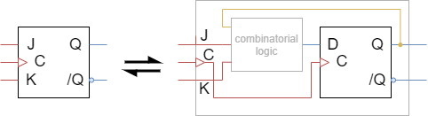
This strategy shall now be used in order to set up a JK flip-flop based on a D flip-flop.
5.2.1 Look onto the problem + Reduce it down to the relevant part
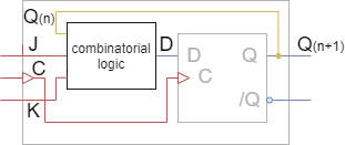
The first step is to take a deeper look onto the problem: The idea is to emulate (or mimic) a JF flip-flop by the use of a D flip-flop and some logic circuit (see figure 17). So the main thing to find is the logic circuit.
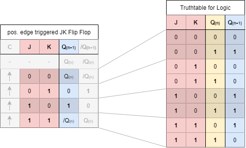
The truthtables of the two flip-flops are shown in figure 18. The relevant (and different) part here is for the rising edge. The other part is similar and does not need further investigation. Since the output $/Q$ always have to be the negation of $Q$, it is only necessary to get the output $Q$ right.
5.2.2 Build up a detailed truth table + look onto the relevant outputs
Now, a full truthtable of the problem has to be filled. In the chapters before, only the external inputs were related to the output. In this case here, the output is also related on the former internal state. For example, the output of JK flip-flop for $J=K=0$ only depends on what the internal state was before.
So now we have to consider the inputs AND the internal states in order to get the output values.
In the figure 19 the truthtable for the JK flip-flop is shown on the left site. The each second line is marked darker for better understanding. On the right site a truthtable is shown, which includes the relation to the internal state.
- For $J=0$ and $K=1$ the output have to be $Q(n+1)=Q=0$ independent from the internal state
- For $J=1$ and $K=0$ the output have to be $Q(n+1)=Q=1$ independent from the internal state
- For $J=0$ and $K=0$ the output will stay the same. Therefore $Q(n+1)=Q(n)$
- For $J=1$ and $K=1$ the output will get inverted. Therefore $Q(n+1)=/Q(n)$
When looking onto this table, one has now to recap, what the main goal is: What does the combinatorical logic in front of the D flip-flop look like?
In figure 20 the circuity of figure 17 is redrawn but now with the input and output variables of the wanted combinatorical logic.
Based on the truthtable of the flip-flop (figure 18) it is clear, that the D flip flop simply delays the output for one cycle.
Therefore, the input $D$ for the D flip-flop is equal to $Q(n+1)$ in figure 19
5.2.3 Fill in and use a Karnaugh map + Create the logic circuit
Based on the truthtable in figure 19 a Karnaugh map can be generated. This is shown in figure 21.
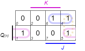
The boolean formula for $D$ is therefore: $D=J\cdot\overline{Q(n)} + Q(n)\cdot \overline{K}$.
With this, the logic circuit can be generated (see figure 22).
5.3 Applications of Flip-Flops
In the previous subchapter a flip-flop was used the substitute a different flip-flop type. Well, that is nice, but what are real applications of flip-flops?
In order to approach this question, first the differences between microcontroller and microprocessor shall be discussed:
A microprocessor is mainly based on the central processing unit (CPU), which processes an incoming data flow. The CPU does this be means of:
- the control unit (CU), which decodes incoming commands.
- the arithmetic logical unit (ALU), which executes commands. Depending on the command sometimes loading and storing relevant data is also necessary.
- some registers. A register is a “specialized byte”, which has major impact in controlling a program. One register ist the program counter, which shows the current position (=address) in the program memory.
The program memory and further specialized logics are not part of the microprocessor.
A microcontroller is based on more parts:
- it contains the CPU, like the microprocessor. Often the CPU of the microprocessor is more lightweight, i.e. it takes less electrical power and is more efficient, but also has less processing power.
- peripherals: Peripherals are dedicated logic which reduced the workload of the CPU. One example is an upcounter, which can be started by the CPU, and runs with a given step width to a given number. Once started the CPU no further processing by th CPU is needed. Further examples are:
- digital I/O (digital input/output): In order to communicate with other ICs, a the data to be transmitted has to be stored, to be send / received bit by bit.
- analog I/O (analog input/output): To analyse analog values an analog-digital-converter (ADC) digitalises the analog values into binary numbers. The other direction is also possible with a digital-to-analog converter.
- interrupt controller: Since the peripherals sometimes still need some interaction - e.g. when the ADC just finished with processing an analog value - a response is needed. Most of the peripherals uses interrupts, which can abruptly stop the CPU in order to jump to a particular code for handling this situation. The interrupt controller is managing these breaks.
- memory: The code is conmmonly stored internally within the microcontroller IC. Often another storage for data is used within the IC. This memory stores the data permanently and is not based on flip-flops.
Nowadays, the microprocessors in computers and mobile devices evolved into “Systems on a Chip” (SoC) which more or less combines microprocessors and microcontrollers. So the still given differences in applications are that
- microprocessors are used for applcations with complex human-machine-interfaces like high resolution graphical user interfaces (GUIs). They also consume more power, have a broad variety of complex commands and often are based on multiple combined CPUs (“multicore”).
- microcontrollers are used for smaller, simpler applications. Here, the price, the low consumption and/or the simple programming is important. Microcontrollers are used in deticated applications, like controlling the ignition in combustion engine cars, or the motor speed of an electric toothbrush. In a mobile device often multiple microcontrollers are included.
But where are flip-flops used there? They are widely used in microcontroller and microprocessors to
- store data,
- delay data,
- count up and down,
- multiply and divide by two, and more specifically double and half a frequency.
In combination with [combinatorial logic] even more complex structures are possible: Virtually all possible outputs with or without an external trigger an be created. This will be more looked onto in detail in the following chapter sequential logic.
Here, the above-mentioned simplier applications will be investigated.
5.3.1 Data Register
A data register can store data based on one or more bits for a distict time within the microprocessor or microcontroller. Usually, the data is stored for multiple clock cycles.
The figure 23 shows a 4-bit data register based on parallel D flip-flops. It can hold the data for one clock cycle. In the shown logic the flip-flops are clocked synchronously: they change their states at the same time based on the clock as a trigger. In the simulation the inputs $X0$…$X3$ can be changed by clicking onto the binary numbers belof the flip-flops.
In order to store the data for longer time, an additional input (e.g. an ENable pin) could deactivate the clock input, when the data has to be stored.
Data registers are used to hold input and output data of the CPU and peripherals.
Exercise 5.3.1. Data Register
Investigate the simulation in figure 23 by toggling the inputs via click on the input value.
- Does the flip-flop act on rising or falling edge?
- The given circuit can only store the data for maximum one step. An idea could be to implement another input $EN$ as an enable pin.
How is this to be connected with the other inputs ($CLK$, $X0$, $X1$, $X2$, $X3$) in order to faciliate an enable pin?
5.3.2 Shift Register
Another register is the shift register. This moves a stored data (e.g. a byte like a=86=0b0101 0110) to the left (0b0010 1011=43) or to the right (0b1010 1100=172). This is used in the CPU to execute the shift C-commands like unsigned int a=b>>2 or unsigned int a=c<<3. Additionally, it enables to multiply or divide by 2, and is also used with the full adder in multiplication algorithms. Furthermore, a shift register can be used for a bit by bit output of an 8bit (or larger) value in communication.
The figure 24 shows a 4-bit shift register based on D flip-flops. In contrast to figure 23 here the flip-flops are connected in serial. Therefore, the output of one flip-flop is the input of the next one, and will be stored in the next clock cycle.
Exercise 5.3.2. Shift Register
Investigate the simulation in figure 24 by toggling the input via click on the input values.
- Open up the simulation in a separate window by
File»Export as Link…»Copy to Clipboardand then<ctrl>+Tplus<ctrl>+V. - What happens when one deletes the input pin and connects the rightmost $/Q$ output to the input?
One application for a shift register is a “short term memory”: In figure 25 the shift register stores the last 4 states of an incoming input bit stream. The logic circuit after the shift register compares the stored data with a given input $X3$…$X0$. Once the exact bit sequence is detected the output switches to $Y=1$.
5.3.3 Frequency Divider
For some applications, only a fraction of the internal clock cycle is necessary. For example, external memory can usually only work with much slower frequencies compared to the CPU. To get a fraction of a given clock frequency a frequency divider can be used.
In figure 26 a 4bit frequency divider based on 4 T flip-flops is shown. Each output of the previous flip-flop is the clock input for the next one. The leftmost flip-flop toggles its output for each rising edge from $0$ to $1$. This expands the $1$ state to the time between two rising edges, similarly with the $0$ state. By this, the time between rising edges is doubled and the frequency is halved.
In contrast to the other two examples, here the flip-flops are clocked asynchronously, i.e. each flip-flop can only start its process when the previous flip-flop finished to output its result $Q$. This adds up the delay given by the propagation delay time $t_{PD}$ step by step. In the figure 26 this can be seen when pushing the Reset button: the rising edge of all flip-flops are not at the same time, but delayed by multiples of $0.5ns$. For slower applications this is might be neglectable, but when multiple flip-flops are used asynchronously the delay will add up and can result in a problematic retardation.
When looking onto the decimal output in figure 26 it seems, that it mostly represents a downcounter. But in detail every second step down and even more every 4th step down (e.g. from 8 to 7) a glitch shows a wrong value shortly. This is due to the above-mentioned delay by the asynchronous flip-flops.
Exercise 5.3.3. Frequency Divider
Investigate the simulation in figure 26.
- Have a look what series the decimal number in the simulation proceed.
- Change the simulation in the following way:
- double click on $CLK$ in order to edit the component and change the frequency to $10MHz$
- increase the
simulation speedwith the slider on the right side - how does the series of the decimal output changes? Does this solve the problem?
The T flip-flop can be emulated with the D flip-flops, by the feedback of $/Q$ to the own input. So, for each next clock cycle, the negated value will be used and therefore the value will toggle. Since the flip-flops are still asynchronous driven (i.e. the clock input is still not triggered with the similar signal) the problems of these frequency divider as a downcounter stills remains the same.
5.3.4 Up-Counter
Counter have multiple applications. One nice appliaction is to get non-binary base fractions from frequencies and more particulary: get a choosable fraction from a frequency.
In order to do so one has to combine the following components (see figure 26):
- an up-counter, which outputs an increasing binary number. This can additionally have a pin to reset the internal state asynchronously.
- a given maximum number in binary, here given by $B$.
- a comparator, which only outputs a $1$ when the inputs $A0$…$A3$ are bit by bit equal to $B0$…$B3$. The output of the comparator is set as an input of the up-counter.
- a toggle flip-flop which only toggles on the rising edge.
In figure 26 also the decimal representation of $A$ and $B$ is shown in order to visualize the process and output. Additionally, also the input $CLK$ and output $Y$ is depict in a timing diagram.
Exercise 5.3.4.1 Up-Counter
Investigate the simulation in figure 28. How does the output $Y$ change, when one changes the input pins given by $B$? Look for the $Y$ in the timing diagram.
So the application is nice, but what does the counter internally look like? How can this counter be generated synchronously with flip-flops? For this a 4bit up-counter based on T flip-flops shall be designed.
Exercise 5.3.4.2 Designing an Up-Counter
The circuit in figure 29 does currently not show a working up-counter. In figure 30 a working up-counter as a blackbox is shown.
- Does some of the outputs $Yn$ already show the correct result? Which one?
- For the outputs $Yn$ which show the wrong results, a different input has to be choosen. Look at the lowest not correct output.
- When does it has to toggle its value?
- Which input are necessary and how can this be implementented into a logic circuit?
- Try to implement the correct logic (only one basic gate is needed)
Examples
In a more functionable version of a register is shown. It has
- the input pins $X7$….$X0$ (pins below the register)
- the output pins $Y7$….$Y0$ (pins on top of the register)
- a clock pin $CLK$ to clock synchronously
- a pin called $LOAD$ which resets the shifting to loading the internal flip flops with the bits given by the inputs. As long as $LOAD=1$ no shifting is made
- a pin called $DIR$ to set the direction. $DIR=0$ leads to right shifting, $DIR=1$ to left shifting.
- a pin called $SIN$ for Serial INput. When right shifting $Y0$ will be set to $SIN$, when left shifting, then $Y7=SIN$
- the output pin $SOUT$ for Serial OUTput
In order to see the register in action set (or reset) $X7$….$X0$, $DIR$ and $SIN$ and then stop the loading with reseting $LOAD$ by $LOAD=0$.
The figure 32 shows the interieur of the register.
Exercises
Exercise 5.4.1. Flip Flops Timing Sequence
The figure 33 shows a series of flip-flops and the $RES$ pin set to 1.
Write down the series of the output $Y0$…$Y3$ for each subsequent cycle of $CLK$, when $RES=0$.