This is an old revision of the document!
4. Basic Circuits II
- Also recommended for basic circuits II is the https://www.ablic.com/en/semicon/products/analog/opamp/intro/
- Operational Amplifiers (Johan Huijsing) [viewable via the university network]
Introductory example
In various applications, currents must be measured. In an electric motor, for example, the torque is caused by the current flowing through the motor. A motor control and also a simple overcurrent shutdown is based on the knowledge of the current. For further processing, a voltage must be generated from the current. The simplest current to voltage converter is the ohmic resistor. A sufficiently large voltage as required by a microcontroller, for example, cannot be achieved with this. So not only the current has to be converted, but also the generated potential difference has to be amplified.
One such current sense amplifier is the INA 240 device. This is installed as shown below. In the simulation, a real current source feeds the electrotechnical image of a DC motor on the left (in the example: inductance with $L_L=10mH$ and internal resistance $R_L=1\Omega$). The current flowing from the motor is conducted through a measuring resistor ($R_M=0.01\Omega$) which is noticeably smaller than the internal resistance of the motor. Thus, most of the power acts in the motor and the current is only marginally affected by the sense resistor. The simulation on the right shows the inner workings of the current measuring amplifier.
The following explains ways in which such circuits can be understood.
Objectives for Basic Circuits II
After this lesson, you should:
- Be able to apply the superpostition method to operational amplifier circuits.
- Know how differential amplifiers and instrumentation amplifiers differ (circuit, applications, advantages and disadvantages).
- Know what the circuit and transfer function of a voltage-to-current converter and current-to-voltage converter look like.
- Be able to name applications for the inverse-radiator, voltage-to-current converter, and current-to-voltage converter.
4.1 Reverse shredder
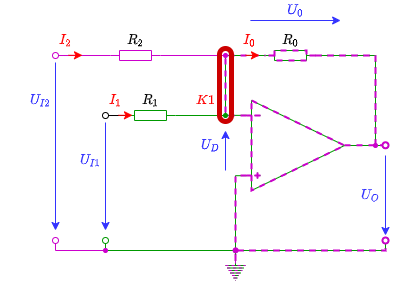
From the inverting amplifier another circuit can be derived, which can be seen in figure 1. Here, both the green part of the circuit and the purple part correspond to an inverting amplifier.
How can $U_A$ be calculated in this circuit? To do this, it is first important to understand what is being sought (compare steps to the goal). The goal is to find the relationship between output and input signals: $U_A(U_{E1}, U_{E2})$. Different ways to get there were explained in Electrical_engineering 1: Analysis of dc_networks. Here we will now outline a different way.
In the case of a circuit with several sources, superposition is a suitable method, in particular the superposition of the effect of all sources in the circuit. For superposition, it must be ensured that the system behaves linearly. The circuit consists of ohmic resistors and the operational amplifier. These two components give twice the output value when the input value is doubled - they behave linearly. For superposition, the effect of the two visible voltage sources $U_{E1}$ and $U_{E2}$ must be analyzed in the present circuit.
In case 1 the voltage source $U_{E1}$ must be considered - the voltage source $U_{E2}$ must be short-circuited for this purpose. The equivalent circuit formed corresponds to an inverting amplifier across $R_2$ and $R_0$. However, there is an additional resistor $R_1$ between the inputs of the operational amplifier. What is the influence of this resistor? The differential voltage $U_D$ between the inputs of the operational amplifier approaches 0. Thus, the following also applies to the current through $R_1$: $I_1^{(1)} \rightarrow 0$. Thus the circuit in case 1 is exactly an inverting amplifier. For case 1, $A_V^{(1)} = \frac{U_A^{(1)}}{U_{E1}} = - \frac{R_0}{R_1}$ and thus: $U_A^{(1)}= - \frac{R_0}{R_1} \cdot U_{E1}$.
Using the same procedure, case 2 for considering the voltage source $U_2$ gives: $U_A^{(2)}= - \frac{R_0}{R_2} \cdot U_{E2}$.
In superposition, the effect results from the addition of partial effects:
$\boxed{U_A = \sum U_A^{(i)} = - (\frac{R_0}{R_2} \cdot U_{E2} + \frac{R_0}{R_1} \cdot U_{E1})}$.
Also, considering the node set for $K1$ in figure 1 gives the same result.
The reverse adder can be extended to any number of inputs. The simulation on the right shows the superposition of several inputs. Depending on the resistances at the different inputs, a different current flows into the circuit.
This circuit was used in analog audio mixers. This allows to combine several signals with different gain (by the input resistors $R_i$ with $i=1, ..., n$). Furthermore, the overall gain can be changed by $R_0$. A big advantage of this circuit is also that the summation at node $K1$ is done on potential $U_D$. This means that capacitive interference with respect to the ground potential is virtually non-existent.
A very similar concept allows the construction of a digital-to-analog converter digital analog converter, DAC.
Exercise 4.1.1 Transfer exercise - signals and systems
- Which mathematical function seems to be visible from the superposition of sinusoidal signals, when these sinusoidal signals double the frequency and halve the amplitude?
(This is the output of the simulation above..) - Which mathematical function seems to be visible in the simulation, when the voltage sources with $80 ~\rm Hz$ and $160 ~\rm Hz$ are removed?
4.2 Differential amplifier / subtractor
In addition to the (reverse) adder, there is also a circuit for subtracting two input values. This circuit became the core of the introductory example. But also in the simulation below this circuit is shown in another example: In this case, a differential input signal is shown on the left. Differential means that the signal on one line is not transmitted with respect to a reference voltage (usually ground potential) on a second line. Instead, the signal is transmitted to both lines in opposite directions. If a disturbance acts equally on both lines (which is often the case when lines are close to each other), the effect of the disturbance can be eliminated by forming the difference.
How can the relationship $U_A(U_{E1}, U_{E2})$ between output and input signals be determined for this circuit?
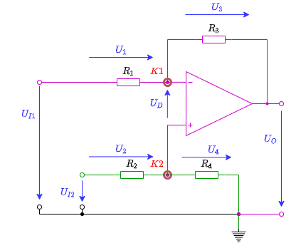
Again, various network analysis concepts could be used to look at the circuit (e.g. superposition or mesh and node sets). Again, another possibility is to split the circuit as color-coded in the figure 2.
The green part shows a voltage divider $R2 + R4$. Since the input resistance of the operational amplifier is very large, this voltage divider is unloaded. The voltage at node $K2$ or at the noninverting input $U_p$ is just given by the voltage divider: $U_p = U_{E2}\cdot \frac{R_4}{R_2+R_4}$.
The violet part corresponds to an inverting amplifier, but the voltage at the node $K1$ or at the inverting input $U_m$ is just equal to $U_p$ due to the feedback, since $U_D \rightarrow \infty$. Thus, the current flowing into node $K1$ via $R_1$ results from $I_1=\frac{U_{E1} - U_p}{R_1}$. The output voltage is given by $U_A = U_p - U_3$, where the voltage $U_3$ is given by the resistance $R_3$ and the current through $R_3$. The current through $R_3$ is just the same as the current through $R_1$, i.e. $I_1$.
The result is:
$U_A = U_{E2}\cdot \frac{R_4}{R_2+R_4} - R_3 \cdot \frac{U_{E1} - U_p}{R_1} $
$U_A= U_{E2}\cdot \frac{R_4}{R_2+R_4} - U_{E1} \cdot \frac{R_3}{R_1} + U_{E2} \cdot (\frac{R_3}{R_1}\cdot \frac{R_4}{R_2+R_4})$
$\boxed{U_A= U_{E2}\cdot \frac{R_4}{R_2+R_4} \frac{R_1+R_3}{R_1} - U_{E1} \cdot \frac{R_3}{R_1}}$
Two simplifications should be considered here:
- If $R_1 = R_2$ and $R_3 = R_4$ are chosen, the equation further simplifies to:
$\boxed{U_A= U_{E2}\cdot \frac{R_3}{R_1} - U_{E1} \cdot \frac{R_3}{R_1} = \frac{R_3}{R_1}\cdot(U_{E2}-U_{E1})}$.
This variant can be found in various measurement circuits.
- Alternatively, if $R_1 = R_3$ and $R_2 = R_4$ is chosen, the result is:
$\boxed{U_A= U_{E2}-U_{E1}}$
This would also result in case 1. if $R_1 = R_2 =R_3 = R_4$ is chosen.
The animation on the right shows how the 2nd case would result with similar triangles. The connection of the two rockers at the point $K_1 K_2$ is caused by the operational amplifier, through which the voltage $U_p$ and $U_m$ converge to $U_D \rightarrow 0$.
A big advantage of this circuit is that even very large voltages can be used as input voltage if $R_1 \gg R_3$ and $R_2 \gg R_4$ are chosen. This would divide the input voltages down and display a fraction of the difference as the result. The main drawback of the circuit is that the gain/attenuation depends on more than one resistor. This makes a quick choice of gain difficult.
4.3 Instrumentation Amplifier
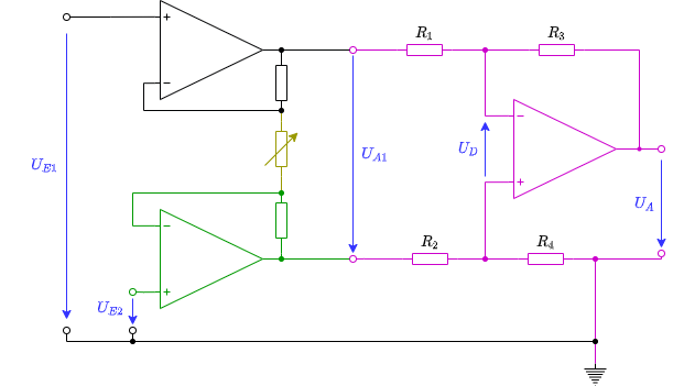
Exercise 4.3.1 Instrumentation amplifier
Find out how the instrumentation amplifier works through internet research.
- Consider the illustrated Falstad Simulation below. What happens when you change the value of the variable resistance?
Analyze especially the minimum and maximum value of the output voltage.
In order to do so, you can start/stop the simulation with theRun/STOPbutton and read the output voltage by moving the mouse pointer over the output signal in the voltage-time diagram. - What happens if you remove the variable resistance and leave the connections open? Which circuit has the OPVs at the entrance?
- Compare the following situations. What is to be determined?
- Variable resistance is replaced by resistance with $2 ~\rm k\Omega$.
- Variable resistance is replaced at the top connection by $1 ~\rm k\Omega$ to mass and lower connection by $1 ~\rm k\Omega$ to mass.
- Variable resistance is replaced at the top connection by $1 ~\rm k\Omega$ to a voltage source with $1 ~\rm V$ and the lower connection also by another $1 ~\rm k\Omega$ to $1 ~\rm V$.
- Which transfer equation $U_{\rm A}=F(U_2, U_1, R_{\rm G}, R)$ does the initial circuit have, when all resistances (except the variable resistance $R_\rm G$) have the same value $R$?
- What are the advantages of the instrumentation amplifier to the differential amplifier?
4.4 Current-Voltage-Converter
In figure 5 you can see the circuit of a current-voltage converter. The current-to-voltage converter changes its output voltage based on an input current. This circuit is also called a transimpedance amplifier because here the transfer resistance - that is, the transimpedance - represents the gain. Generally, the gain was expressed as $$A={ {output} \over {input} }$$. In the case of the current-to-voltage converter, the gain is defined as.
$$R = {{U_{out}} \over I_{in}} = - R_1$$
$R_1$ is the resistor used in the circuit.
In the simulation, the slider on the right (“Current of current source”) can be varied. This changes the input current and thus also the output voltage.
This circuit can be used, for example, to read a photodiode in volt-free circuit (further explanation and integrated circuit tsl250r.pdf).
4.5 Voltage-to-Current Converter
Next, consider the voltage-to-current converter. With this, an output current is set proportional to an input voltage.
Here, the general gain $$A={ {output} \over {input} }$$ to
$$S ={{I_{out}} \over U_{in}}$$
The quantity $S$ is called the transmission slope or the transmission conductance.
This circuit can be used, for example, to generate a voltage-regulated current source.
Tasks
Further Reading
Learning Questions
- State applications for the reverse adder.
- Explain the working of a current to voltage converter.
- Name 3 applications for an operational amplifier.


