Übungsblatt 4
Bitte laden Sie das aufgefüllte PDF in ILIAS hoch.
Details, Tipps und Tools zum Ausfüllen und Einfügen von Bildern finden Sie unter:
Tools für Lehr/Lern-Veranstaltungen
| Name | Vorname | Matrikelnummer |
|---|---|---|
| $\quad\quad\quad\quad\quad\quad\quad\quad$ | $\quad\quad\quad\quad\quad\quad\quad\quad$ | $\quad\quad\quad\quad\quad\quad\quad\quad$ |
| |
Exercise 3.3.1 Analysis of the impedance converter circuit with different operational amplifiers
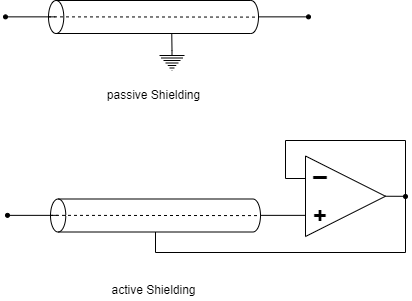
Imagine that you work in the company “HHN Mechatronics & Robotics”, which is a cheap mobile EKG – So you want to build a measuring device for the electrocardiogram or the cardiac voltage curve - for athletes and those in need. The measurement signal has only a few millivolts and microamps. In order to protect the signal from electromagnetic radiation on the way from the glued-on electrode to the evaluation electronics, a electromagnetic shielding placed around the line (see figure 1, above). However, since this creates a parasitic capacitor, a colleague suggested active shielding. The shielding is always kept at the measuring voltage that is applied to the line via a voltage follower (see figure 1, under). The parasitic capacitor is never charged due to this structure, since the same voltage prevails on both sides - there is no falsification of the signal. It is important for the application that the voltage follower reacts quickly.
You are supervised with the design of this voltage follower and should use the available operational amplifiers $\rm LM318$, $\rm uA741$, and $\rm uA776$ analyze in the voltage follower circuit.
Write a short report (problem description, circuit in TINA TI, results, discussion) and use TINA TI for the solution.
- Recreate the circuit described above for a realistic operational amplifier in Tina. Use a voltage generator as a source unit step with the amplitude $U_\rm A = 1.0 ~\rm V$.
- Simulate over
Analysis»Transient…the time course for the specified operational amplifiers.
Determine the time that elapses until the initial value of $0.1 ~\rm V$ for the first time $0.9 ~\rm V$ achieved ($10~\rm %$ to $90 ~\rm %$ of the amplitude, too. It is called rise time). - Describe the passage of time in each case. Are there any other differences besides the rise time?
- Based on the information provided, which of the three op amps would you choose for the problem?
In-depth information (not relevant to the exercise):
- Detailed description of a EMG/EKG Vorverstärkerschaltung
Exercise 3.5.1 inverting amplifier
1. Derive the voltage gain $A_{\rm V}= {{U_{\rm O}}\over{U_{\rm I}}}$ for the inverting amplifier.
Use the procedure that was used for the non-inverting amplifier.
- What is looking for?
- Number of variables?
- Number of necessary equations?
- Establishing the known equations
- Derivation of the voltage gain
Take into account that for the differential gain $A_\rm D$ of the ideal OPV applies: $A_\rm D \rightarrow \infty$. And the following also applies: $1/A_\rm D \rightarrow 0$
But the following doesn't always apply: ${{C}\over{U_x \cdot A_\rm D}} \rightarrow 0$, for an unknown constant $C$ and a voltage $U_x$!
2. Which type of amplifier circuit (inverting or non-inverting amplifier) has the lower input resistance? Why?
Exercise 3.5.2. Variations of the non-inverting amplifier
Below you will find circuits with an ideal operational amplifier, which are similar to the non-inverting amplifier and whose voltage gain $A_V$ must be determined.
Assumptions
- $R_1 = R_3 = R_4 = R$
- $R_2 = 2 \cdot R$
- $U_\rm I$ comes from a low-resistance source
- $U_\rm O$ is due to a high-resistance consumer
Exercises
- Enter the voltage gain $A_\rm V$ for each circuit. A detailed calculation as before is not necessary.
- For Figure 7, indicate how the voltage gain can be determined.
- Generalize with the following justifications:
- How has a short circuit of the two OPV inputs must be taken into account?
- How do resistances have to be considered in the following cases:
- with one terminal (so “one connector”) directly and exclusively on an OPV input,
- with both terminals each directly connected to an OPV input.
- In which circuits do resistors $R_3$ and $R_4$ represent an unloaded voltage divider?
To approach the problems, you should try to use the knowledge from the inverting amplifier. It can be useful to simulate the circuits via Falstad-Circuit or Tina TI. In the first two circuits, tips can be seen under the illustration as support.
Important: As always in your studies, you should try to generalize the knowledge gained from the task.
Tipps
- How big is the current flow into the inverting and non-inverting input of an ideal operational amplifier? So what voltage drop would there be across a resistor whose one connection only leads to one input of the operational amplifier ($R_3$)?
- The operational amplifier always tries to output as much current at the output that the required minimum voltage $U_\rm D$ results between the inverting and non-inverting input. How high can $U_\rm D$ be assumed? Can this voltage also be built up via a resistor ($R_4$)?
- Can different resistors (e.g. because they are between the same nodes) be combined?
Abb. 1

Abb. 2

Abb. 3

Abb. 4

Abb. 5

Abb. 6

Abb. 7

Abb. 8

Abb. 9
