Advanced simulations
Junction Field Effect Transistor (JFET)
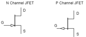
The structure of the junction field effect transistor (JFET) resembles the bipolar transistor at first glance. In Abbildung 1, the individual images (1)…(3) show the layering of an n-channel (English n-channel) JFET and the circuit symbol in the upper left. In contrast to the pnp bipolar transistor, however, here the p-doped layers are jointly supplied with voltage and the n-doped layer is transversely fluxed. Without voltage difference $U_{GS}$ between gate and source, a (small) junction is formed at the p-n junctions. Electrons can flow unhindered through the n-doped layer: a current $I_G \gg 0$ flows through the FET (Abbildung 1 Fig. (1)). The „path“ between the two junction layers is called the n-channel.

When the voltage difference $U_{GS}$ becomes smaller than zero, the junction layers increase, and the diode between G and S is operated in the reverse direction. The n-channel is constricted and geometrically decreases the electron or current flow $I_G$ (Abbildung 1 Fig. (2)). At a certain voltage $U_{GS}=U_p$ (pinch-off or pinch-off voltage), the two junction layers are so large that no n-channel is left - the channel is pinched-off** (Abbildung 1 figure (3)). Above this voltage, there can be no current flow. The principle is thus similar to the situation when the flow from a water hose is regulated by squeezing the hose.
In the simulation on the right, the same voltage ratios are shown. The toggle switch on the left makes it possible to invert the voltage $U_{DS}$ via the transistor. If this becomes negative, a slightly different situation arises: The JFET seems to become conductive in all, regardless of what voltage $U_{GS}$ assumes.
~CLEARFIX~~
Digital Analogue Converter (DAC)
In chapter 3, a digital-to-analog converter was described in task 3.5.3. The R-2R ladder described there allows a pure digital value to be output as an analog voltage as an integrated circuit. In the simulation on the right a simplified version can be seen. However, the simplified version requires many very precisely tuned resistors. In contrast, the R-2R ladder requires only 2 resistor values and this is easier to manufacture in terms of microsystem technology.
~PAGEBREAK~ ~CLEARFIX~~
Time Domain - Frequency Domain
arbitrary periodic signals
At the previous chapter a sinusoidal input voltage was used for the analysis. How do the filters work Here we want to focus on it again.
In Abbildung 3 it can be seen that a square wave signal can be approximated by several sinusoidal signals. If the amplitudes of these signals are plotted versus frequency, an image of the signal in the frequency domain is obtained. This transformation is done computationally via the Fourier transform and is treated in detail in advanced subjects such as control engineering, signals and systems and digital signal processing.
For very fast changes, high-frequency components are required.
Already with the Umkehraddierer it became apparent that a periodic sawtooth signal can be assembled from several sinusoidal voltages.
~CLEARFIX~~~


From the sinus
The video But what is a Fourier series? explains clearly how even vector images can be generated by superimposing sine functions.