This is an old revision of the document!
Block 11 — Influence and displacement field
Learning objectives
- …
Preparation at Home
Well, again
- read through the present chapter and write down anything you did not understand.
- Also here, there are some clips for more clarification under 'Embedded resources' (check the text above/below, sometimes only part of the clip is interesting).
For checking your understanding please do the following exercises:
- …
90-minute plan
- Warm-up (x min):
- ….
- Core concepts & derivations (x min):
- …
- Practice (x min): …
- Wrap-up (x min): Summary box; common pitfalls checklist.
Conceptual overview
- …
Core content
Electric Field inside of a conductor
As seen in Block10, any hole inside a conductor does neither show field lines nor an electric field. This is called Faraday cage or Faraday shield.
Wo we want to have a look onto an uncharged object in an external field. Also here any hole inside does not show an electric field
The reason for that is, that the outer field gets cancelled out by an opposing inner electric field.
A charge displacement on the external surface (induced by the external field) is the reason for that opposing inner field.
Please have a look onto the yellow and blue collor in figure 1 to see this charge displacement

Note:
Any external electric field causes a charge displacement on an conductor in such a way, that there in no internal field inside the material (neither in holes nor in the material itself)Electrostatic Induction
In a thought experiment, an uncharged conductor (e.g., a metal plate) is brought into an electrostatic field (figure 2).
The external field or the resulting Coulomb force causes the moving charge carriers to be displaced.
Fig. 2: Viewing the induced charge separation

Results:
- The charge carriers are still distributed on the surface.
- Now, equilibrium is reached when just so many charges have moved, that the electric field inside the conductor disappears (again).
- The field lines leave the surface again at right angles. Again, a parallel component would cause a charge shift in the metal.
This effect of charge displacement in conductive objects by an electrostatic field is referred to as electrostatic induction (in German: Influenz). Induced charges can be separated (figure 2 right). If we look at the separated induced charges without the external field, their field is again just as strong in magnitude as the external field only in the opposite direction.
Note:
- The location of an induced charge is always on the conductor surface. This results in a surface charge density $\varrho_A = {{\Delta Q}\over{\Delta A}}$
- The conductor surface in the electrostatic field is always an equipotential surface. Thus, the field lines always originate and terminate perpendicularly on conductor surfaces.
- The interior of the conductor is always field-free (Faraday effect: metallic enclosures shield electric fields).
How can the conductor surface be an equipotential surface despite different charges on both sides? Equipotential surfaces are defined only by the fact that the movement of a charge along such a surface does not require/produce a change in energy. Since the interior of the conductor is field-free, movement there can occur without a change in energy. As the potential between two points is independent of the path between them, a path along the surface is also possible without energy expenditure.
Electric Field inside of an Isolator
But how is it like for an isolator in an external field?
There are no free charges in an isolator - so, is there no compensation of the external field inside the isolator at all?
The simulation in figure 4 shows something different: it looks like, that ther is some compensation but not a complete one.

So, let us look into an isolator: The figure 5 shows a scetch of the inner of an isolator in an electric field.
Most of the isolators have a bipolar property (e.g. water): Its material consists of units, which are partially positively charged and partially negatively charged. This units cannot move, but they might get bend and rotated. This induces some charges on the surface, and these compensate some of the electric field by an oppositing field.

So the root-cause-path is:
- We have initially the external electric field.
- This induces the counteracting field by bending the dipoles.
- The internal measurable electric field is compensated
To have an uncompensated field in the following the electric displacement flux density $\vec{D}$ is introduced. The electric displacement flux density is only focusing on the cause of the electric fields. As we have seen, its effect can differ since the space can also “hinder” the electric field in an effect.
The electric displacement flux density is only related to the causing charges $Q$. Thie relationship is shown in the following.
\begin{align} \boxed{Q = \int {\rm d}Q = {\rlap{\rlap{\int_A} \int} \: \LARGE \circ} \vec{D} \cdot {\rm d} \vec{A} } \end{align}
The symbol ${\rlap{\Large \rlap{\int} \int} \, \LARGE \circ}$ denotes that there is a closed surface used for the integration.
The meaning of the formula is: The “sum” of the $D$-field emanating over the surface is thus just as large as the sum of the charges contained therein, since the charges are just the sources of this field.
This can be compared with a bordered swamp area with water sources and sinks:
- The sources in the marsh correspond to the positive charges, and the sinks to the negative charges. The formed water corresponds to the $D$-field.
- The sum of all sources and sinks equals, in this case, just the water stepping over the edge.

Dielectric strength of dielectrics
- The dielectrics act as insulators. The flow of current is therefore prevented
- The ability to insulate is dependent on the material.
- If a maximum electric field $E_0$ is exceeded, the insulating ability is eliminated.
- One says: The insulator breaks down. This means that above this electric field, a current can flow through the insulator.
- Examples are: Lightning in a thunderstorm, ignition spark, glow lamp in a phase tester
- The maximum electric field $E_0$ is referred to as dielectric strength (in German: Durchschlagfestigkeit or Durchbruchfeldstärke).
- $E_0$ depends on the material (see table 2), but also on other factors (temperature, humidity, …).
Common pitfalls
- …
Exercises
Tasks
Task 5.4.1 Simulation
In the simulation in figure 9, the equipotential lines and electric field at different objects can be represented. In the beginning, the situation of an infinitely long cylinder in a homogeneous electric field is shown. The solid lines show the equipotential surfaces. The small arrows show the electric field.
- What is the angle between the field on the surface of the cylinder?
- Once the option
Flat Viewis deactivated, an alternative view of this situation can be seen. Additionally, charged test particles can be added withDisplay: Particles (Vel.). This alternative view looks similar to what other physical fields? - What can be said about the potential distribution on the cylinder?
- On the left half of the field lines enter the body, on the right half, they leave the body. What can be said about the charge carrier distribution at the surface? Check also the representation
Floor: charge! - Is there an electric field inside the body?
- Is this cylinder metallic, semiconducting, or insulating?
Task 5.4.2 electrical Field at different Geometry I (exam task, ca 6% of a 60 minute exam)

The figure on the right shows an arrangement of ideal metallic conductors (gray) with specified charge. In white a dielectric (e.g. vacuum) is shown. Several designated areas are shown by green dashed frames, which are partly inside the objects.
Arrange the designated areas clearly according to ascending field strength (magnitude)! Indicate also, if designated areas have quantitatively the same field strength.
- What is the field in a room completely surrounded by a conductive conductor?
- How does the field behave inside a conductor?
- Does the field strength increase or decrease when a charge moves away from another charge?
- Is the field at a peak higher or lower?
- At $b$ and $d$ no field is measurable, because the surrounded conductor is on a constant field. There is no potential difference and therefore no field.
- At $c$ a field (magnitude >0) is measurable, which points from the charge ($+1~\rm{C}$) to the elongated conductor ($-2~\rm{C}$). Due to the tip, there is an excess charge and thus a higher field.
- At $a$ a field (magnitude >0) is measurable, which points from the charge ($+1~\rm{C}$) to the elongated conductor ($-2~\rm{C}$).
Task 5.4.3 electrical Field at different Geometry II (exam task, ca 6 % of a 60 minute exam)

The figure on the right shows an arrangement of ideal metallic conductors (gray) with specified charge. In white a dielectric (e.g. vacuum) is shown. Several designated areas are shown by green dashed frames, which are partly inside the objects.
Arrange the designated areas clearly according to ascending field strength (magnitude)! Indicate also, if designated areas have quantitatively the same field strength.
Task 5.4.4 electrical Field at different Geometry II (exam task, ca 6% of a 60 minute exam)

The figure on the right shows an arrangement of ideal metallic conductors (gray) with specified charge. In white a dielectric (e.g. vacuum) is shown. Several designated areas are shown by green dashed frames, which are partly inside the objects.
Arrange the designated areas clearly according to ascending field strength (magnitude)! Indicate also, if designated areas have quantitatively the same field strength.
Task 5.4.5 Simulation
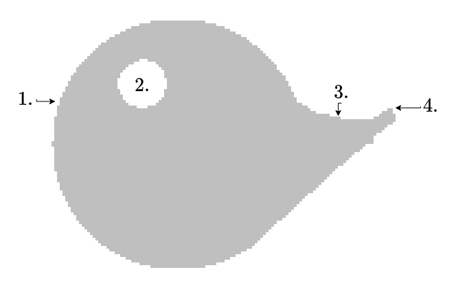
Given is the two-dimensional component shown in figure 10. The component shall be charged positively.
In the picture, there are 4 positions marked with numbers.
Order the numbered positions by increasing charge density!
Task 5.5.1 induced Charges
A plate capacitor with a distance of $d = 2 ~{ \rm cm}$ between the plates and with air as dielectric ($\varepsilon_{ \rm r}=1$) gets charged up to $U = 5~{ \rm kV}$. In between the plates, a thin metal foil with the area $A = 45~{ \rm cm^2}$ is introduced parallel to the plates.
Calculate the amount of the displaced charges in the thin metal foil.
- What is the strength of the electric field $E$ in the capacitor?
- Calculate the displacement flux density $D$
- How can the charge $Q$ be derived from $D$?
Task 5.5.2 Manipulating a Capacitor I
An ideal plate capacitor with a distance of $d_0 = 7 ~{ \rm mm}$ between the plates gets charged up to $U_0 = 190~{ \rm V}$ by an external source. The source gets disconnected. After this, the distance between the plates gets enlarged to $d_1 = 7 ~{ \rm cm}$.
- What happens to the electric field and the voltage?
- How does the situation change (electric field/voltage), when the source is not disconnected?
- Consider the displacement flux through a surface around a plate
- $U_1 = 1.9~{ \rm kV}$, $E_1 = 27~{ \rm kV/m}$
- $U_1 = 190~{ \rm V}$, $E_1 = 2.7~{ \rm kV/m}$
Task 5.5.3 Manipulating a Capacitor II
An ideal plate capacitor with a distance of $d_0 = 6 ~{ \rm mm}$ between the plates and with air as dielectric ($\varepsilon_0=1$) is charged to a voltage of $U_0 = 5~{ \rm kV}$. The source remains connected to the capacitor. In the air gap between the plates, a glass plate with $d_{ \rm g} = 4 ~{ \rm mm}$ and $\varepsilon_{ \rm r} = 8$ is introduced parallel to the capacitor plates.
1. Calculate the partial voltages on the glas $U_{ \rm g}$ and on the air gap $U_{ \rm a}$.
- Build a formula for the sum of the voltages first
- How is the voltage related to the electric field of a capacitor?
The sum of the voltages across the glass and the air gap gives the total voltage $U_0$, and each individual voltage is given by the $E$-field in the individual material by $E = {{U}\over{d}}$: \begin{align*} U_0 &= U_{\rm g} + U_{\rm a} \\ &= E_{\rm g} \cdot d_{\rm g} + E_{\rm a} \cdot d_{\rm a} \end{align*}
The displacement field $D$ must be continuous across the different materials since it is only based on the charge $Q$ on the plates. \begin{align*} D_{\rm g} &= D_{\rm a} \\ \varepsilon_0 \varepsilon_{\rm r, g} \cdot E_{\rm g} &= \varepsilon_0 \cdot E_{\rm a} \end{align*}
Therefore, we can put $E_\rm a= \varepsilon_{\rm r, g} \cdot E_\rm g $ into the formula of the total voltage and rearrange to get $E_\rm g$: \begin{align*} U_0 &= E_{\rm g} \cdot d_{\rm g} + \varepsilon_{\rm r, g} \cdot E_{\rm g} \cdot d_{\rm a} \\ &= E_{\rm g} \cdot ( d_{\rm g} + \varepsilon_{\rm r, g} \cdot d_{\rm a}) \\ \rightarrow E_{\rm g} &= {{U_0}\over{d_{\rm g} + \varepsilon_{\rm r, g} \cdot d_{\rm a}}} \end{align*}
Since we know that the distance of the air gap is $d_{\rm a} = d_0 - d_{\rm a}$ we can calculate: \begin{align*} E_{\rm g} &= {{5'000 ~\rm V}\over{0.004 ~{\rm m} + 8 \cdot 0.002 ~{\rm m}}} \\ &= 250 ~\rm{{kV}\over{m}} \end{align*}
By this, the individual voltages can be calculated: \begin{align*} U_{ \rm g} &= E_{\rm g} \cdot d_\rm g &&= 250 ~\rm{{kV}\over{m}} \cdot 0.004~\rm m &= 1 ~{\rm kV}\\ U_{ \rm a} &= U_0 - U_{ \rm g} &&= 5 ~{\rm kV} - 1 ~{\rm kV} &= 4 ~{\rm kV}\\ \end{align*}
2. What would be the maximum allowed thickness of a glass plate, when the electric field in the air-gap shall not exceed $E_{ \rm max}=12~{ \rm kV/cm}$?
Now we shall eliminate $E_\rm g$, since $E_\rm a$ is given in the question. \begin{align*} U_0 &= E_{\rm g} \cdot d_{\rm g} + E_{\rm a} \cdot d_{\rm a} \\ &= {{E_\rm a}\over{\varepsilon_{\rm r,g}}} \cdot d_{\rm g} + E_{\rm a} \cdot d_{\rm a} \\ \end{align*}
The distance $d_\rm a$ for the air is given by the overall distance $d_0$ and the distance for glass $d_\rm g$: \begin{align*} d_{\rm a} = d_0 - d_{\rm g} \end{align*}
This results in: \begin{align*} U_0 &= {{E_{\rm a}}\over{\varepsilon_{\rm r,g}}} \cdot d_{\rm g} + E_{\rm a} \cdot (d_0 - d_{\rm g}) \\ {{U_0}\over{E_{\rm a} }} &= {{1}\over{\varepsilon_{\rm r,g}}} \cdot d_{\rm g} + d_0 - d_{\rm g} \\ &= d_{\rm g} \cdot ({{1}\over{\varepsilon_{\rm r,g}}} - 1) + d_0 \\ d_{\rm g} &= { { {{U_0}\over{E_{\rm a} }} - d_0 } \over { {{1}\over{\varepsilon_{\rm r,g}}} - 1 } } &= { { d_0 - {{U_0}\over{E_{\rm a} }} } \over { 1 - {{1}\over{\varepsilon_{\rm r,g}}} } } \end{align*}
With the given values: \begin{align*} d_{\rm g} &= { { 0.006 {~\rm m} - {{5 {~\rm kV} }\over{ 12 {~\rm kV/cm}}} } \over { 1 - {{1}\over{8}} } } &= { {{8}\over{7}} } \left( { 0.006 - {{5 }\over{ 1200}} } \right) {~\rm m} \end{align*}
Task 5.5.4 Spherical capacitor
Two concentric spherical conducting plates set up a spherical capacitor. The radius of the inner sphere is $r_{ \rm i} = 3~{ \rm mm}$, and the inner radius from the outer sphere is $r_{ \rm o} = 9~{ \rm mm}$.
- What is the capacity of this capacitor, given that air is used as a dielectric?
- What would be the limit value of the capacity when the inner radius of the outer sphere goes to infinity ($r_{ \rm o} \rightarrow \infty$)?
- What is the displacement flux density of the inner sphere?
- Out of this derive the strength of the electric field $E$
- What ist the general relationship between $U$ and $\vec{E}$? Derive from this the voltage between the spheres.
- $C = 0.5~{ \rm pF}$
- $C_{\infty} = 0.33~{ \rm pF}$
Task 5.5.5 Applying Gauss's law: Electric Field of a line charge
Embedded resources
Application of electrostatic induction: Protective bag against electrostatic charge/discharge