Table of Contents
2 Simple DC circuits
So far, only simple circuits consisting of a source and a load connected by wires have been considered.
In the following, more complicated circuit arrangements will be analyzed. These initially contain only one source, but several lines and many ohmic loads (cf. figure 1).

2.1 Idealized Components
Learning Objectives
By the end of this section, you will be able to:
- Know the representation of ideal current and voltage sources in the U-I diagram.
- Know the internal resistance of ideal current and voltage sources.
- Know the symbol of ideal current and voltage sources.
- Know the properties of ideal resistance and ideal connection.
Every electrical circuit consists of three elements:
- Consumers also called Loads (in German: Verbraucher or Last): consumers convert electrical energy into energy that is not purely electrical.
e.g.- into electrostatic energy (capacitor)
- into magnetostatic energy (magnet)
- into electromagnetic energy (LED, light bulb)
- into mechanical energy (loudspeaker, motor)
- into chemical energy (charging an accumulator)
- Sources also called Generator (in German: Quellen): sources convert energy from another form of energy into electrical energy. (e.g. generator, battery, photovoltaic).
- Wires also called Interconnections (in German Leitungen or Verbindungen): The wires of interconnection lines link consumers to sources.
These elements will be considered in more detail below.
Consumer
- The colloquial term 'consumer' in electrical engineering stands for an electrical consumer - i.e. a component that converts electrical energy into another form of energy.
- A resistor is often also referred to as a consumer. In addition to pure ohmic consumers, however, there are also ohmic-inductive consumers (e.g. coils in a motor) or ohmic-capacitive consumers (e.g. various power supplies using capacitors at the output). Correspondingly the equation “consumer is a resistor” is wrong.
- Current-voltage characteristics (see figure 2)
- Current-voltage characteristics of a load always run through the origin, because without current there is no voltage, and vice versa.
- Ohmic loads have a linear current-voltage characteristic which can be described by a single numerical value.
The slope in the $U$-$I$-characteristic is the conductance: $I = G \cdot U = {{U}\over{R}}$

Sources
- Sources act as generators of electrical energy
- A distinction is made between ideal and real sources.
The real sources are described in the following chapter “non-ideal_sources_and_two_terminal_networks”.
The ideal voltage source generates a defined constant output voltage $U_\rm s$ (in German often $U_\rm q$ for Quellenspannung).
In order to maintain this voltage, it can supply any current.
The current-voltage characteristic also represents this (see figure 3).
The circuit symbol shows a circle with two terminals. In the circuit, the two terminals are short-circuited.
Another circuit symbol shows the negative terminal of the voltage source as a “thick minus symbol”, the positive terminal is drawn wider.
The ideal current source produces a defined constant output current $I_\rm s$ (in German often $I_\rm q$ for Quellenstrom).
For this current to flow, any voltage can be applied to its terminals.
The current-voltage characteristic also represents this (see figure 4).
The circuit symbol shows again a circle with two connections. This time the two connections are left open in the circle and a line is drawn perpendicular to them.


Another Explanation of Ideal Sources
Wire Connection
- The ideal connection line is resistance-free and transmits current and voltage instantaneously.
- Real existing influences (e.g. voltage drop) of connections are considered via separately drawn components (e.g. ohmic resistance).
2.2 Reference-Arrow Systems, Sign Convention, and first Consideration of a DC Circuit
Learning Objectives
By the end of this section, you will be able to:
- apply and distinguish between the producer and consumer reference arrow systems (German: Erzeuger-Pfeilsystem und Verbraucher-Pfeilsystem).
- similarly use passive and active sign conventions.
In the chapter 1. Preparation and Proportions the direction of conventional current and voltages has already been discussed. Unfortunately, with meshed networks it is often not clear ahead of the calculation in which direction the conventional sense of direction of all currents and voltages runs.
In figure 5 such a meshed net is shown. In this circuit, a switch $S_1$ and a current $I_2$ are marked. Once the state of the switch is swapped, the direction of the current changes.
Sign and Arrow-Systems
For the direction of the arrows different conventions are available. Here (and quite often in Germany) the convention of power engineering is used. This convention is
Generator Reference Arrow System / Active Sign Convention

With sources (or generators), energy is taken from the environment and made available to the circuit.
For generators, the arrowfoot of the current is attached to the arrowhead of the voltage. Voltage and current arrows are antiparallel ($\uparrow \downarrow$).
Similarly, the active sign convention for one component states: The current enters the component on the more negative terminal. Or vice versa: The current exits the component on the positive terminal.
Both expressions “generator arrow system” and “active sign convention” come to the same result, when drawing the arrows.
For generators holds: $P_{1} = U_{12} \cdot I_1 \stackrel{!}{>} 0$
The power transfer from the environment to the power system via the generator or the generator arrow system is calculated positively.

Load Reference Arrow System
In the case of consumers, energy is taken from the circuit and made available to the environment.
For consumers, the arrowfoot or arrowhead of the current and voltage are related. Voltage and current arrows are parallel ($\uparrow \uparrow$).
Here we have to use the passive sign convention: The current enters the component on the more positive terminal. Or vise versa: The current exits the component on the negative terminal.
Both expressions again come to the same result, when drawing the arrows.
For consumers, the following holds:
$P_{3} = U_{34} \cdot I_3 \stackrel{!}{>} 0$
The power transfer from the power system to the environment via the consumer or the consumer arrow system is also calculated positively.
Note:
- Before the calculation, the reference arrows for currents and voltages are set arbitrarily, with the following conditions:
- the active sign convention/generator arrow system is used for all sources (e.g. all voltage and current sources): the current is antiparallel to the voltage arrow.
- the passive sign convention/motor arrow system is used for all consumers (e.g. all passives like resistors, capacitors, inductors, diodes, etc.): the current is parallel to the voltage arrow.
- for loads, where the direction of the power is not known, the motor arrow system is recommended (e.g. passives, in case these are part of a machine, like inductors of a motor)
- After the calculation means
- $I>0$: The reference arrow reflects the conventional directional sense of the current
- $I<0$: The reference arrow points in the opposite direction to the conventional directional sense of the current
- Reference arrows of the current are drawn in the wire if possible.

The reference arrow system (in the clip '+' and '-' is shown in the component terminal.
We will instead use voltage arrows from plus to minus
2.3 Nodes, Branches, and Loops
Explanation of the different network structures
(Graphs and trees are only needed in later chapters)
Learning Objectives
By the end of this section, you will be able to:
- identify the nodes, branches, and loops in a circuit.
- use them to reshape a circuit.
Electrical circuits typically have the structure of networks. Networks consist of two elementary structural elements:
- Branches (German: Zweige): Connections between two nodes.
- Node (German: Knoten): Connection “point” of several branches.

Please note in the case of electrical circuits, we will use the following definition:
- Branches contain at least one component.
- Nodes connect more than two branches. Since the wire in a circuit diagram is an ideal conductor, all connected wires to a node are at the same voltage level. Therefore the node in the circuit diagram can also be spatially extended by the wires.

Sometimes there is a differentiation between “simple nodes” (only connecting 2 branches) and “principal nodes” (connecting more than 2 branches). We will in the following often only mark the connection of more than two branches with a node.
Branches in electrical networks are also called two-terminal networks. Their behavior is described by current-voltage characteristics and explained in more detail in the chapter non-ideal_sources_and_two_terminal_networks.
In addition, another term is to be explained:
A loop is a closed path in the loop. This means that a loop begins and ends at the same node and runs over at least one further node.
Since a voltmeter can also be present as a component between two nodes, it is also possible to close a loop by a drawn voltage arrow (cf. $U_1$ in figure 10).
A loop that does not contain other (smaller) loops is called a mesh.
Please keep in mind, that usually the entire behavior of networked circuits almost always changes when a change occurs in one branch or at one node. This is in contrast to other cause-effect relationships, but comparable to changes in other larger networks, e.g. a traffic jam in the road network, due to which other roads experience a higher load. For electrical engineering, this means that in the case of changing circuits, the focus is often on determining the interrelationships (formulas, current-voltage characteristics) and not on a single numerical value.
Reshaping Circuits
With the knowledge of nodes, branches, and meshes, circuits can be simplified. Circuits can be reshaped arbitrarily as long as all branches remain at the same nodes after reshaping The figure 11 shows how such a transformation is possible.

For practical tasks, repeated trial and error can be useful. It is important to check afterward that the same components are connected to each node as before the transformation.
Further examples can be found in the following video
Exercise 2.3.1 Branches and Nodes

For the markings in the circuits in figure 12 indicate whether it is a branch, a node, or neither.
Exercise 2.3.2 Branches and Nodes (with explanation)
Exercise 2.3.3 Reshaping circuits

Reshape the circuits in figure 13.
2.4 Kirchhoff's Circuit Laws
Learning Objectives
By the end of this section, you will be able to: Know and apply Kirchhoff's circuit laws (Kirchhoff's current law and Kirchhoff's voltage law).
Kirchhoff's Current Law
Kirchhoff's current law (Kirchhoff's first law, Kirchhoff's nodal rule, in German: Knotensatz) formulates in the language of mathematics the experience that no charge “accumulations” occur in electrical wires. This is of particular relevance at a network node (figure 14). To formulate the equation at this node, the reference arrows of the currents are all set in the same way. That means: all point away from or towards the node.
Note:

The sum of all currents flowing from the nodes must be zero.
$\boxed{I_1 + I_2 + I_3 + ... + I_n = \sum_{x=1}^{n} I_x=0}$
From now on, the following definition applies:
- Currents whose current arrows point towards the node are added to the calculation.
- Currents whose current arrows point away from the node are subtracted in the calculation.
Parallel circuit of resistors
From Kirchhoff's current law, the total resistance for resistors connected in parallel can be derived (figure 15):

Since the same voltage $U_{ab}$ is dropped across all resistors, using Kirchhoff's current law:
$\large{{U_{ab}}\over{R_1}}+ {{U_{ab}}\over{R_2}}+ ... + {{U_{\rm ab}}\over{R_n}}= {{U_{\rm ab}}\over{R_{\rm eq}}}$
$\rightarrow \large{{{1}\over{R_1}}+ {{1}\over{R_2}}+ ... + {{1}\over{R_n}}= {{1}\over{R_{\rm eq}}} = \sum_{x=1}^{n} {{1}\over{R_x}}}$
Thus, for resistors connected in parallel, the equivalent conductance $G_{\rm eq}$ (German: Ersatzleitwert) is the sum of the individual conductances: $G_{\rm eq} = \sum_{x=1}^{n} {G_x}$
In general: the equivalent resistance of a parallel circuit is always smaller than the smallest resistance.
Especially for two parallel resistors $R_1$ and $R_2$ applies: $R_{\rm eq}= \large{{R_1 \cdot R_2}\over{R_1 + R_2}}$
Current divider
Derivation of the current divider with examples
The current divider rule shows in which way an incoming current on a node will be divided into two outgoing branches.
The rule states that the currents $I_1, ... I_n$ on parallel resistors $R_1, ... R_n$ behave just like their conductances $G_1, ... G_n$ through which the current flows.
$\large{{I_1}\over{I_{\rm res}} = {{G_1}\over{G_{\rm res}}}$
$\large{{I_1}\over{I_2}} = {{G_1}\over{G_2}}$
The rule also be derived from Kirchhoff's current law:
- The voltage drop $U$ on parallel resistors $R_1, ... R_n$ is the same.
- When $U_1 = U_2 = ... = U$, then the following equation is also true: $R_1 \cdot I_1 = R_2 \cdot I_2 = ... = R_{\rm eq} \cdot I_{\rm res}$.
- Therefore, we get with the conductance: ${{I_1} \over {G_1}} = {{I_2} \over {G_2}}= ... = {{I_{\rm eq}} \over {G_{\rm res}}}$
Exercise 2.4.1 Current divider
In the simulation in figure 16 a current divider can be seen. The resistances are just inversely proportional to the currents flowing through it.
- What currents would you expect in each branch if the input voltage were lowered from $5~\rm V$ to $3.3V~\rm $? After thinking about your result, you can adjust the
Voltage(bottom right of the simulation) accordingly by moving the slider. - Think about what would happen if you flipped the switch before you flipped the switch.
After you flip the switch, how can you explain the current in the branch?
Exercise 2.4.2 two resistors
Two resistors of $18~\Omega$ and $2~\Omega$ are connected in parallel. The total current of the resistors is $3~\rm A$.
Calculate the total resistance and how the currents are split to the branches.
Kirchhoff's Voltage Law
Also, Kirchhoff's voltage law (also called: Kirchhoff's second law, or loop law) describes in mathematical language another practical experience: Between two points $1$ and $2$ of a network, there is only one potential difference. Thus the potential difference is in particular independent of the way a network is traversed between the two points $1$ and $2$. This can be described by considering the meshes.
Note:

In any mesh of an electrical circuit, the sum of all voltages is always zero (figure 17):
$\boxed{U_{1} + U_{2} + ... + U_{n} = \sum_{x=1}^{n} U_x = 0}$
To calculate this, a convention for the loop direction must be specified. Theoretically, this can be chosen arbitrarily. In practice, often a specific direction (e.g. clockwise) is used.
Independently, the following specification always applies: For voltage drop, the inverse sign of a voltage rise has to be taken into account.
For example:
- Voltages, whose voltage arrows point in the direction of circulation are added in the calculation.
- Voltages, whose voltage arrows point against the direction of rotation are subtracted in the calculation.
Proof of Kirchhoff's voltage law
If one expresses the voltage in figure 17 by the potentials in the nodes, we get:
$U_{12}= \varphi_1 - \varphi_2 $
$U_{23}= \varphi_2 - \varphi_3 $
$U_{34}= \varphi_3 - \varphi_4 $
$U_{41}= \varphi_4 - \varphi_1 $
If these voltages are added, this leads to Kirchhoff's voltage law.
$U_{12}+U_{23}+U_{34}+U_{41} = 0$
Series circuit of resistors

Using Kirchhoff's voltage law, the total resistance of a series circuit (in German: Reihenschaltung, see figure 18) can be easily determined:
$U_1 + U_2 + ... + U_n = U_{\rm res}$
$R_1 \cdot I_1 + R_2 \cdot I_2 + ... + R_n \cdot I_n = R_{\rm eq} \cdot I $
Since in a series circuit, the current through all resistors must be the same - i.e. $I_1 = I_2 = ... = I$ - it follows that:
$R_1 + R_2 + ... + R_n = R_{\rm eq} = \sum_{x=1}^{n} R_x $
In general: The equivalent resistance of a series circuit is always greater than the greatest resistance.
Application
Kelvin-Sensing
Often resistors are used to measure a current $I$ via the voltage drop on the resistor $U = R \cdot I$. Applications include the measurement of motor currents in the range of $0.1 ... 500 ~\rm A$.
Those resistors are called shunt resistors and are commonly in the range of some $\rm m\Omega$.
This measurement can be interfered by the resistor of the supply lines.
To get an accurate measurement often Kelvin sensing, also known as Four-terminal sensing or 4 wire sensing, is used.
This is a method of measuring electrical resistance avoiding errors caused by wire resistances.
The simulation in figure 19 shows such a setup.
Four-terminal sensing involves using:
- a pair of current leads or force leads (with the resistances $R_{\rm cl1}$ and $R_{\rm cl2}$) to supply current to the circuit and
- a pair of voltage leads or sense leads (with the resistances $R_{\rm vl1}$ and $R_{\rm vl2}$) to measure the voltage drop across the impedance to be measured.
The sense connections via the voltage leads are made immediately adjacent to the target impedance $R_{\rm s}$ at the device under test $\rm DUT$.
By this, they do not include the voltage drop in the force leads or contacts.
Since almost no current flows to the measuring instrument, the voltage drop in the sense leads is negligible.
This method can be a practical tool for finding poor connections or unexpected resistance in an electrical circuit.
Exercise 2.4.3 Three Resistors
Three equal resistors of $20~k\Omega$ each are given.
Which values are realizable by the arbitrary interconnection of one to three resistors?
2.5 Voltage Divider
Why are voltage dividers important? (a cutout from 0:00 to 10:56 from a full video of EEVblog, starting from 17:00 there is also a nice example for troubles with voltage dividers..)
The unloaded Voltage Divider
Learning Objectives
By the end of this section, you will be able to:
- to distinguish between the loaded and unloaded voltage divider.
- to describe the differences between loaded and unloaded voltage dividers.
Especially the series circuit of two resistors $R_1$ and $R_2$ shall be considered now. This situation occurs in many practical applications e.g. in a potentiometer.

In figure 21 this circuit is shown.

Via Kirchhoff's voltage law, we get
$\boxed{ {{U_1}\over{U}} = {{R_1}\over{R_1 + R_2}} \rightarrow U_1 = k \cdot U}$
The ratio $k={{R_1}\over{R_1 + R_2}}$ also corresponds to the position on a potentiometer.
Exercise 2.5.1 unloaded voltage divider
In the simulation in figure 22 an unloaded voltage divider in the form of a potentiometer can be seen. The ideal voltage source provides $5~\rm V$. The potentiometer has a total resistance of $1~\rm k\Omega$. In the configuration shown, this is divided into $500 ~\Omega$ and $500 ~\Omega$.
- What voltage $U_{\rm O}$ would you expect if the switch were closed? After thinking about your result, you can check it by closing the switch.
- First, think about what would happen if you would change the distribution of the resistors by moving the wiper (“intermediate terminal”).
You can check your assumption by using the slider at the bottom right of the simulation. - At which position do you get a $U_{\rm O} = 3.5~\rm V$?
The loaded Voltage Divider
If - in contrast to the abovementioned, unloaded voltage divider - a load $R_{\rm L}$ is connected to the output terminals (figure 23), this load influences the output voltage.

A circuit analysis yields:
$ U_1 = \LARGE{{U} \over {1 + {{R_2}\over{R_L}} + {{R_2}\over{R_1}} }}$
or on a potentiometer with $k$ and the sum of resistors $R_{\rm s} = R_1 + R_2$:
$ U_1 = \LARGE{{k \cdot U} \over { 1 + k \cdot (1-k) \cdot{{R_{\rm s}}\over{R_{\rm L}}} }}$
figure 24 shows the ratio of the output voltage $U_1$ to the input voltage $U$ (y-axis), in relation to the ratio $k={{R_1}\over{R_1 + R_2}}$. In principle, this is similar to figure 21, but here it has another dimension: multiple graphs are plotted. These differ by the ratio ${{R_{\rm s}}\over{R_{\rm L}}}$.
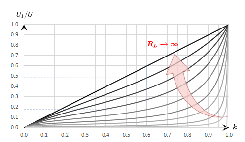
What does this diagram tell us? This shall be investigated by an example. First, assume an unloaded voltage divider with $R_2 = 4.0 ~\rm k\Omega$ and $R_1 = 6.0 ~\rm k\Omega$, and an input voltage of $10~\rm V$. Thus $k = 0.60$, $R_s = 10~\rm k\Omega$ and $U_1 = 6.0~\rm V$. Now this voltage divider is loaded with a load resistor. If this is at $R_{\rm L} = R_1 = 10 ~\rm k\Omega$, $k$ reduces to about $0.48$ and $U_1$ reduces to $4.8~\rm V$ - so the output voltage drops. For $R_{\rm L} = 4.0~\rm k\Omega$, $k$ becomes even smaller to $k=0.375$ and $U_1 = 3.75~\rm V$. If the load $R_{\rm L}$ is only one-tenth of the resistor $R_{\rm s}=R_1 + R_2$, the result is $k = 0.18$ and $U_1 = 1.8~\rm V$. The output voltage of the unloaded voltage divider ($6.0~\rm V$) thus became less than one-third.
What is the practical use of the (loaded) voltage divider?
Here are some examples:
- Voltage dividers are in use for controlling the output of power supply ICs (see Voltage Dividers in Power Supplies). In order not to create a loaded voltage divider, a range for the resistance is given here.
- Another “invisible” voltage divider is for example in the electrical system of a car. As we will learn in the next chapters, voltage supplies have internal resistance (and therefore batteries, too). The other consumer in the car also represents a resistance. By this, the electrical system states an unloaded voltage divider. Given another, additional low-resistance load (e.g. the spark or the starter motor of the starter system) one can understand that there will be a voltage drop when starting the car.
Exercise 2.5.2 loaded voltage divider I
Determine from the circuit in figure 23 the equation $ U_1 = {{k \cdot U} \over { 1 + k \cdot (1-k) \cdot{{R_{\rm s}}\over{R_{\rm L}}}}}$ where $k={{R_1}\over{R_1 + R_2}}$ and $R_{\rm s} = R_1 + R_2$.
Exercise 2.5.3 loaded voltage divider II
In the simulation in figure 25 a loaded voltage divider in the form of a potentiometer can be seen. The ideal voltage source provides $5.00~\rm V$. The potentiometer has a total resistance of $1.00~k\Omega$. In the configuration shown, this is divided into $500 ~\Omega$ and $500 ~\Omega$. The load resistance has $R_{\rm L} = 1.00 ~\rm k\Omega$.
- What voltage
U_Owould you expect if the switch were closed? This is where you need to do some math! After you calculated your result, you can check it by closing the switch. - At which position of the wiper do you get $3.50~\rm V$ as an output? Determine the result first by means of a calculation.
Then check it by moving the slider at the bottom right of the simulation.
Exercise 2.5.4 Application of the loaded voltage divider - motor

You wanted to test a micromotor for a small robot. Using the maximum current and the internal resistance ($R_{\rm M} = 5~\Omega$) you calculate that this can be operated with a maximum of $U_{\rm M, max}=4~\rm V$. A colleague said that you can get $4~\rm V$ using the setup in figure 26 from a $9~\rm V$ block battery.
- First, calculate the maximum current $I_{\rm M,max}$ of the motor.
- Draw the corresponding electrical circuit with the motor connected as an ohmic resistor.
- At the maximum current, the motor should be able to deliver a torque of $M_{\rm max}=M(I_{\rm M, max})= 100~\rm mNm$. What torque would the motor deliver if you implement the setup like this? (Assumption: The torque of the motor increases proportionally to the motor current).
- What might a setup with a potentiometer look like that would actually allow you to set a voltage between $0.5~\rm V$ to $4~\rm V$ on the motor? What resistance value should the potentiometer have?
- Build and test your circuit in the simulation below. For an introduction to online simulation, see: online_circuit_simulator.
You will essentially need the following tips for this setup:- Routing connections can be activated via the menu:
Draw»add wire. Afterward, you have to click on the start point and then drag it to the end mode. - Note that connections can only ever be connected at nodes. A red-marked node (e.g. at the $5 ~\Omega$ resistor) indicates that it is not connected. This could be moved one grid step to the left, as there is a node point there.
- Pressing the
<ESC>key will disable the insertion of components. - With a right click on a component it can be copied or values like the resistor can be changed via
Edit….
Exercise 2.5.5 Examples of the calculation of loaded voltage dividers
Exercise on the voltage divider
Exercise 2.5.6 Example of a loaded voltage divider: Explanation without calculation (German)
2.6 Circuits with three Connections
Learning Objectives
By the end of this section, you will be able to:
- convert triangular loops into a star shape (and vice versa)
At the beginning of the chapter, an example of a network was shown (figure 1). Here, however, one does not come directly to the solution with the set of nodes and loops. It is visible, that there are many $\Delta$-shaped (or triangle-shaped) loops resp. $\rm Y$-shaped (or star-shaped) nodes, see figure 28. A method to calculate these will be discussed in more detail now.
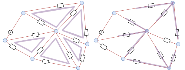
First of all a summary of the previous findings: Using the node and loop rule it became clear that an equivalent resistance can be determined from a series as well as from a parallel circuit. If one considers the equivalent resistance as a black box - i.e. the internals are unknown - it could be interpreted by both types of a circuit (figure 29).
Now how does this help us in the case of a $\Delta$-load (= triangular loop)?
Also in this case one can provide a black box. However, this should always behave in the same way as the $\Delta$-load, i.e. any voltages applied should produce the same currents as the known structure.
In other words: The resistances measured between two terminals must be identical for the black box and for the known circuit.
For this purpose, the different resistances between the individual nodes $\rm a$, $\rm b$, and $\rm c$ are now to be considered, see figure 30. The aim is to find out how a $\Delta$-load (triangular circuit) can be developed from a $\rm Y$-load (star circuit) and vice versa.
Fig. 30: Star-delta transformation
Calculation of the transformation formulae: Star connection in delta connection (Alternatively in German)
Delta Circuit
In the delta circuit, the 3 resistors $R_{\rm ab}^1$, $R_{\rm bc}^1$, and $R_{\rm ca}^1$ are connected in a loop. At the connection of the resistors, an additional terminal is implemented.
The labeling with a superscript $\square^1$ refers to the three resistors in the next paragraphs.
For the measurable resistance between two terminals (e.g. $R_{\rm ab}$ between $\rm a$ and $\rm b$), the third terminal (here: $\rm c$) is considered as not connected to anything outside. This results in a parallel circuit of the direct delta resistor $R_{\rm ab}^1$ with the series connection of the other two delta resistors $R_{\rm ca}^1 + R_{\rm bc}^1$:

$R_{\rm ab} = R_{\rm ab}^1 || (R_{\rm ca}^1 + R_{\rm bc}^1) $
$R_{\rm ab} = {{R_{\rm ab}^1 \cdot (R_{\rm ca}^1 + R_{\rm bc}^1)}\over{R_{\rm ab}^1 + (R_{\rm ca}^1 + R_{\rm bc}^1)}} = {{R_{\rm ab}^1 \cdot (R_{\rm ca}^1 + R_{\rm bc}^1)}\over{R_{\rm ab}^1 + R_{\rm ca}^1 + R_{\rm bc}^1}} $
The same applies to the other connections. This results in:
\begin{align*} R_{\rm ab} = {{R_{\rm ab}^1 \cdot (R_{\rm ca}^1 + R_{\rm bc}^1)}\over{R_{\rm ab}^1 + R_{\rm ca}^1 + R_{\rm bc}^1}} \\ R_{\rm bc} = {{R_{\rm bc}^1 \cdot (R_{\rm ab}^1 + R_{\rm ca}^1)}\over{R_{\rm ab}^1 + R_{\rm ca}^1 + R_{\rm bc}^1}} \\ R_{\rm ca} = {{R_{\rm ca}^1 \cdot (R_{\rm bc}^1 + R_{\rm ab}^1)}\over{R_{\rm ab}^1 + R_{\rm ca}^1 + R_{\rm bc}^1}} \tag{2.6.1} \end{align*}
Star Circuit
Given the idea, that the star circuit shall behave equally to the delta circuit, the resistance measured between the terminals must be similar. Also in the star circuit, 3 resistors are connected, but now in a star (or $\rm Y$) shape. The star resistors are all connected with another node $0$ in the middle: $R_{\rm a0}^1$, $R_{\rm b0}^1$ and $R_{\rm c0}^1$.
Again, the procedure is the same as for the delta connection: the resistance between two terminals (e.g. $\rm a$ and $\rm b$) is determined, and the further terminal ($\rm c$) is considered to be open. The resistance of the further terminal ($R_{\rm c0}^1$) is only connected at one node. Therefore, no current flows through it - it is thus not to be considered. It results in:
\begin{align*} R_{\rm ab} = R_{\rm a0}^1 + R_{\rm b0}^1 \\ R_{\rm bc} = R_{\rm b0}^1 + R_{\rm c0}^1 \\ R_{\rm ca} = R_{\rm c0}^1 + R_{\rm a0}^1 \tag{2.6.2} \end{align*}
From equations $(2.6.1)$ and $(2.6.2)$ we get:
\begin{align} R_{\rm ab} = {{R_{\rm ab}^1 \cdot (R_{\rm ca}^1 + R_{\rm bc}^1)}\over{R_{\rm ab}^1 + R_{\rm ca}^1 + R_{\rm bc}^1}} = R_{\rm a0}^1 + R_{\rm b0}^1 \tag{2.6.3} \end{align} \begin{align} R_{\rm bc} = {{R_{\rm bc}^1 \cdot (R_{\rm ab}^1 + R_{\rm ca}^1)}\over{R_{\rm ab}^1 + R_{\rm ca}^1 + R_{\rm bc}^1}} = R_{\rm b0}^1 + R_{\rm c0}^1 \tag{2.6.4} \end{align} \begin{align} R_{\rm ca} = {{R_{\rm ca}^1 \cdot (R_{\rm bc}^1 + R_{\rm ab}^1)}\over{R_{\rm ab}^1 + R_{\rm ca}^1 + R_{\rm bc}^1}} = R_{\rm c0}^1 + R_{\rm a0}^1 \tag{2.6.5} \end{align}
Equations $(2.6.3)$ to $(2.6.5)$ can now be cleverly combined so that there is only one resistor on one side.
A variation is to write the formulas as ${{1}\over{2}} \cdot \left( (2.6.3) + (2.6.4) - (2.6.5) \right)$ or ${{1}\over{2}} \cdot \left(R_{\rm ab} + R_{\rm bc} - R_{\rm ca}\right)$ to combine. This gives $R_{\rm b0}^1$
\begin{align*} {{1}\over{2}} \cdot \left( {{R_{\rm ab}^1 \cdot (R_{\rm ca}^1 + R_{\rm bc}^1)}\over{R_{\rm ab}^1 + R_{\rm ca}^1 + R_{\rm bc}^1}} + {{R_{\rm bc}^1 \cdot (R_{\rm ab}^1 + R_{\rm ca}^1)}\over{R_{\rm ab}^1 + R_{\rm ca}^1 + R_{\rm bc}^1}} - {{R_{\rm ca}^1 \cdot (R_{\rm bc}^1 + R_{\rm ab}^1)}\over{R_{\rm ab}^1 + R_{\rm ca}^1 + R_{\rm bc}^1}} \right) &= {{1}\over{2}} \cdot \left( R_{\rm a0}^1 + R_{\rm b0}^1 + R_{\rm b0}^1 + R_{\rm c0}^1 - R_{\rm c0}^1 - R_{\rm a0}^1 \right) \\ {{1}\over{2}} \cdot \left( {{R_{\rm ab}^1 \cdot (R_{\rm ca}^1 + R_{\rm bc}^1)} + {R_{\rm bc}^1 \cdot (R_{\rm ab}^1 + R_{\rm ca}^1)} - {R_{\rm ca}^1 \cdot (R_{\rm bc}^1 + R_{\rm ab}^1)}\over{R_{\rm ab}^1 + R_{\rm ca}^1 + R_{\rm bc}^1}} \right) &= {{1}\over{2}} \cdot \left( 2 \cdot R_{\rm b0}^1 \right) \\ {{1}\over{2}} \cdot \left( {{R_{\rm ab}^1 R_{\rm ca}^1 + R_{\rm ab}^1 R_{\rm bc}^1 + R_{\rm bc}^1 R_{\rm ab}^1 + R_{\rm bc}^1 R_{\rm ca}^1 - R_{\rm ca}^1 R_{\rm bc}^1 - R_{\rm ca}^1 R_{\rm ab}^1}\over{R_{\rm ab}^1 + R_{\rm ca}^1 + R_{\rm bc}^1}} \right) &= R_{\rm b0}^1 \\ {{1}\over{2}} \cdot \left( {{ 2 \cdot R_{\rm ab}^1 R_{\rm bc}^1 }\over{R_{\rm ab}^1 + R_{\rm ca}^1 + R_{\rm bc}^1}} \right) &= R_{\rm b0}^1 \\ {{ R_{\rm ab}^1 R_{\rm bc}^1 }\over{R_{\rm ab}^1 + R_{\rm ca}^1 + R_{\rm bc}^1}} &= R_{\rm b0}^1 \\ \end{align*}
Similarly, one can resolve to $R_{\rm a0}^1$ and $R_{\rm c0}^1$, and with a slightly modified approach to $R_{\rm ab}^1$, $R_{\rm bc}^1$ and $R_{\rm ca}^1$.
Y-Δ-Transformation
Notice:
If a delta circuit is to be converted into a star circuit, the star resistors can be determined via:
\begin{align*} \color{lightgray}{\boxed{ \color{black}{\begin{array}{} \text{star resistance} \\ \text{at the terminal x} \end{array} }}} &= {{ \color{lightgray}{\boxed{ \color{black}{\begin{array}{} \text{product of} \\ \text{the delta resistances} \\ \text{connected with x} \end{array} }}} } \over { \color{lightgray}{\boxed{ \color{black}{\begin{array}{} \text{sum of all} \\ \text{delta resistances} \end{array} }}}}} \\ \\ \text{therefore:}\quad\quad\quad\quad\quad\quad R_{\rm a0}^1 &= {{ R_{\rm ca}^1 \cdot R_{\rm ab}^1 }\over{R_{\rm ab}^1 + R_{\rm ca}^1 + R_{\rm bc}^1}} \\ R_{\rm b0}^1 &= {{ R_{\rm ab}^1 \cdot R_{\rm bc}^1 }\over{R_{\rm ab}^1 + R_{\rm ca}^1 + R_{\rm bc}^1}} \\ R_{\rm c0}^1 &= {{ R_{\rm bc}^1 \cdot R_{\rm ca}^1 }\over{R_{\rm ab}^1 + R_{\rm ca}^1 + R_{\rm bc}^1}} \end{align*}
If a star circuit is to be converted into a delta circuit, the star resistors can be determined via:
\begin{align*} \color{lightgray}{\boxed{ \color{black}{\begin{array}{} \text{delta resistance} \\ \text{between the} \\ \text{terminals x and y} \end{array} }}} &= {{ \color{lightgray}{\boxed{ \color{black}{\begin{array}{} \text{sum of all} \\ \text{products between} \\ \text{varying star resistances} \end{array} }}} } \over { \color{lightgray}{\boxed{ \color{black}{\begin{array}{} \text{star resistance} \\ \text{opposite x and y} \end{array} }}}}} \\ \\ \text{therefore:}\quad\quad\quad\quad\quad\quad R_{\rm ab}^1 &= {{ R_{\rm a0}^1 \cdot R_{\rm b0}^1 +R_{\rm b0}^1 \cdot R_{\rm c0}^1 +R_{\rm c0}^1 \cdot R_{\rm a0}^1 }\over{ R_{\rm c0}^1}} \\ R_{\rm bc}^1 &= {{ R_{\rm a0}^1 \cdot R_{\rm b0}^1 +R_{\rm b0}^1 \cdot R_{\rm c0}^1 +R_{\rm c0}^1 \cdot R_{\rm a0}^1 }\over{ R_{\rm a0}^1}} \\ R_{\rm ca}^1 &= {{ R_{\rm a0}^1 \cdot R_{\rm b0}^1 +R_{\rm b0}^1 \cdot R_{\rm c0}^1 +R_{\rm c0}^1 \cdot R_{\rm a0}^1 }\over{ R_{\rm b0}^1}} \end{align*}
Exercise 2.6.1 Application of delta-Y conversion
Exercise 2.6.2 more difficult exercise with Y-delta transformation (German)
2.7 Circuits with multiple Resistors
Learning Objectives
By the end of this section, you will be able to:
- simplify circuits consisting only of resistors.
- calculate the voltages and currents in circuits with a voltage source and several resistors.
- simplify symmetrical circuits.
In this subchapter, a methodology is discussed, which should help to reshape circuits. In subchapter 2.6 Star-Delta-Circuit towards the end a network was already transformed in a way, that it does not contain triangular meshes anymore. Now, this procedure shall be systematized. Starting points are tasks, where for a resistor network the total resistance, total current, or total voltage has to be calculated.
Simple Example
An example of such a circuit is given in figure 32. Here $I_0$ is wanted. This current can be found by the (given) voltage $U_0$ and the total resistance between the terminals $\rm a$ and $\rm b$. So we are looking for $R_{\rm ab}$.

As already described in the previous subchapters, partial circuits can also be converted into equivalent resistors step by step. It is important to note that these partial circuits for conversion into equivalent resistors may only ever have two connections (= two nodes to the “outside world”).

figure 33 shows the step-by-step conversion of the equivalent resistors in this example.
As a result of the equivalent resistance one gets:
\begin{align*} R_{\rm eq} = R_{12345} &= R_{12}||R_{345} = R_{12}||(R_3+R_{45}) = (R_1||R_2)||(R_3+R_4||R_5) \\ &= {{ {{R_1 \cdot R_2}\over{R_1 + R_2}} \cdot (R_3 + {{R_4 \cdot R_5}\over{R_4 + R_5}}) }\over{ {{R_1 \cdot R_2}\over{R_1 + R_2}} +R_3 + {{R_4 \cdot R_5}\over{R_4 + R_5}} }} \quad \quad \quad \quad \quad \quad \bigg\rvert \cdot{{(R_1 + R_2) \cdot (R_4 + R_5)}\over{(R_1 + R_2) \cdot (R_4 + R_5)}} \\ &= {{ R_1 \cdot R_2 \cdot (R_3 + {{R_4 \cdot R_5}\over{R_4 + R_5}}) \cdot (R_4 + R_5) } \over { R_1 \cdot R_2\cdot(R_4 + R_5) +R_3 + R_4 \cdot R_5 \cdot (R_1 + R_2)}} \\ &= {{ R_1 \cdot R_2 \cdot (R_3 \cdot (R_4 + R_5) + R_4 \cdot R_5) } \over { R_1 \cdot R_2\cdot(R_4 + R_5) +R_3 + R_4 \cdot R_5 \cdot (R_1 + R_2)}} \\ \end{align*}
Example of Δ-Y-Transformation
With the Δ-Y-transformation now also the initial example can be transformed. For more complicated circuits, the repeated Δ-Y-transformation with a subsequent combining of the resistors is useful, until the resulting circuit is easily calculable with node and mesh theorem (figure 34). Here a calculation is omitted - it is recommended to calculate here with intermediate results for the transformed resistors.
Fig. 34: example circuit conversion

Example with Symmetries in the Circuit
A certain special case concerns possible symmetries in circuits. If these are present, further simplification can be made.
Fig. 35: Example with symmetries in the circuit
figure 35 shows on the left a symmetrical construction of a network of equal resistors $R$. For better understanding, in the middle of the same circuit, additional switches and test points (TP) are installed, which indicate the voltage to the ground.
The switches can be used to check whether a current flows if the respective nodes are connected. In the simulation, it can be seen that this is not the case. In the symmetrical setup, these nodes are each at the same potential.
This also allows the circuit to take the form shown in figure 35 on the right. This circuit is again easy to calculate:
\begin{align*} R_{\rm eq} = R || R + R || R || R || R + R || R || R || R + R || R = {{1}\over{2}}\cdot R + {{1}\over{4}}\cdot R + {{1}\over{4}}\cdot R + {{1}\over{2}}\cdot R = 1.5\cdot R \end{align*}
Exercise 2.7.1 Circuit Simplification Exercise I (in German)
Exercise 2.7.2 Circuit Simplification Exercise II + III (in German)
Exercise 2.7.3 Circuit Simplification Exercise IV (in German)
Exercise 2.7.4 Circuit Simplification Exercise V (in German)
Exercise 2.7.5 Circuit Simplification Exercise VI (in German)
Exercise 2.7.6 Circuit Simplification VII Exercise (in German)
Exercise 2.7.7 Simplifying Circuits (exam task, about 8% of a 60-minute exam, WS2020)

Given is the adjoining circuit with
$R_1=10 ~\Omega$
$R_2=20 ~\Omega$
$R_3=5 ~\Omega$
and the switch $S$.
1. Determine the total resistance $R_{\rm eq}$ between A and B by summing the resistances with the switch $S$ open.
- How can the circuit be better represented or pulled apart?
- The switch should be replaced by an open wire in this case.
For this purpose, the individual branches can be highlighted in color and interpreted as a “conductive rubber band”.
This results in:


Thus $R_3$ and $R_3$ can be combined to $R_{33} = 2 \cdot R_3 = R_1$, yielding a left and a right voltage divider.
Now it is visible that in the left and right voltage divider, the same potential is at the respective branch, or at the node K1 (green) and K2 (pink).
Thus, the total resistance can be calculated as $R_{\rm eq} = (2 \cdot R_1)||(2 \cdot R_1)$.
However, by symmetry, nodes K1 and K2 can also be short-circuited. Thus, $R_{\rm eq} = 2 \cdot \left( R_1||R_1 \right)$ also holds.
2. What is the total resistance when switch $S$ is closed?
So the resistance remains the same.
Exercise 2.7.8: Simplifying Circuits II (written exam task, approx 8% of a 60-minute written exam, WS2020)

Given is the adjoining circuit with
$R_1=5 ~\Omega$
$R_2=10 ~\Omega$
$R_3=20 ~\Omega$
1. Determine the equivalent resistance $R_{\rm eq}$ between A and B by summing the resistances.
- How can the circuit be better represented or pulled apart?
- Switches (when used) should be replaced by an open or closed circuit.
- Does this result in equal potentials at different nodes that can be cleverly used?
For this purpose, the individual branches can be highlighted in color and interpreted as a “conductive rubber band”.
It can be seen that the two resistors $R_3$ at the top left and bottom right are each shorted. The result is thus:


Here it helps to consider the potential of the nodes K1, K2, and K3. For K2, the resistances $R_2 || R_3 || R_2$ must be combined at the top and bottom. Thus, the same resistance values at the top and bottom result. Also at the nodes K1 and K2 the same resistance values at the top and at the bottom result. With the same ratios of the resistances at K1, K2, and K3 respectively, it can be concluded that no current flows across the resistors $R_3$ between K1 and K2 or K2 and K3. Thus, these do not contribute to the total resistance. In such a case, a short circuit or an open line can be freely chosen between the relevant nodes for the calculation. In the following, an open line is chosen. Additionally, the parallel strings can be reordered.
This results in:

\begin{align*} R_{\rm eq} &= \left( \left( 2 \cdot R_2 \right) || \left( 2 \cdot R_2 \right) \right) && || \; \left( \left( 2 \cdot R_3 \right) || \left( 2 \cdot R_3 \right) || \left( 2 \cdot R_3 \right) \right) \\ R_{\rm eq} &= R_2 && || \;\left( R_3 || \left( 2 \cdot R_3 \right) \right) \\ R_{\rm eq} &= R_2 && || \;\frac{R_3 \cdot 2 R_3}{R_3 + 2 R_3} \\ R_{\rm eq} &= R_2 && || \;\frac{2}{3}\cdot R_3 \\ R_{\rm eq} &= \frac{R_2 \cdot \frac{2}{3}\cdot R_3}{R_2 + \frac{2}{3}\cdot R_3} \\ R_{\rm eq} &= \frac{R_2 \cdot R_3}{\frac{3}{2}\cdot R_2 + R_3} \\ \\ \end{align*}
2. Now let the voltage from A to B be: $U_{AB}=U_0= 20 ~\rm V$. What is the current $I$?
Exercise 2.7.9 - Variation: Simplifying Circuits II (written exam task, approx 8% of a 60-minute written exam, WS2020)

Given is the adjoining circuit with
$R_1=10 ~\Omega$
$R_2=20 ~\Omega$
$R_3=5 ~\Omega$
1. Determine the equivalent resistance $R_{\rm eq}$ between A and B by summing the resistances.
2. Now let the voltage from A to B be: $U_{\rm AB}=U_0= 10 ~\rm V$. What is the current $I$?
Exercise 2.7.10 - Variation: Simplifying Circuits III (written exam task, approx 8% of a 60-minute written exam, WS2020)

Given is the adjoining circuit with
$R_1=5 ~\Omega$
$R_2=20 ~\Omega$
$R_3=10 ~\Omega$
1. Determine the equivalent resistance $R_{\rm eq}$ between A and B by summing the resistances.
2. Now let the voltage from A to B be: $U_{\rm AB}=U_0= 30 ~\rm V$. What is the current $I$?
Exercise 2.7.11 - Simplifying symmetric Circuits
well explained example of a simplification due to symmetry: